©2011 Silicon Storage Technology, Inc. DS25080A 11/11
13
2 Mbit SPI Serial Flash
SST25LF020A
Not Recommended for New Designs
A
Microchip Technology Company
Sector-Erase
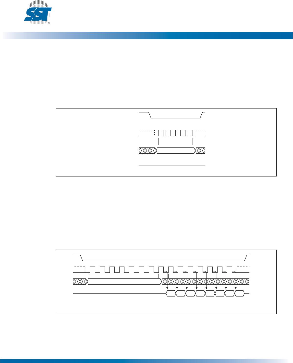
The Sector-Erase instruction clears all bits in the selected 4 KByte sector to FFH. A Sector-Erase
instruction applied to a protected memory area will be ignored. Prior to any Write operation, the Write-
Enable (WREN) instruction must be executed. CE# must remain active low for the duration of the any
command sequence. The Sector-Erase instruction is initiated by executing an 8-bit command, 20H, fol-
lowed by address bits [A
23
-A
0
]. Address bits [A
MS
-A
12
](A
MS
= Most Significant address) are used to
determine the sector address (SA
X
), remaining address bits can be V
IL
or V
IH.
CE# must be driven high
before the instruction is executed. The user may poll the Busy bit in the software status register or wait
T
SE
for the completion of the internal self-timed Sector-Erase cycle. See Figure 9 for the Sector-Erase
sequence.
Figure 9: Sector-Erase Sequence
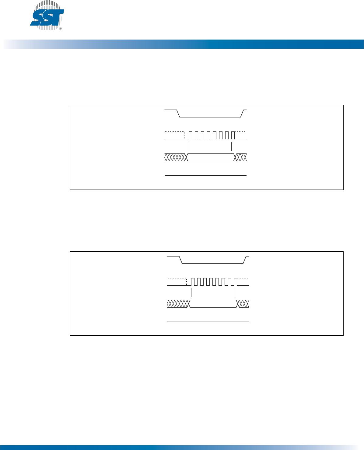
Block-Erase
The Block-Erase instruction clears all bits in the selected 32 KByte block to FFH. A Block-Erase
instruction applied to a protected memory area will be ignored. Prior to any Write operation, the Write-
Enable (WREN) instruction must be executed. CE# must remain active low for the duration of any com-
mand sequence. The Block-Erase instruction is initiated by executing an 8-bit command, 52H, followed
by address bits [A
23
-A
0
]. Address bits [A
MS
-A
15
](A
MS
= Most significant address) are used to deter-
mine block address (BA
X
), remaining address bits can be V
IL
or V
IH
. CE# must be driven high before the
instruction is executed. The user may poll the Busy bit in the software status register or wait T
BE
for the com-
pletion of the internal self-timed Block-Erase cycle. See Figure 10 for the Block-Erase sequence.
Figure 10: Block-Erase Sequence
CE#
SO
SI
SCK
ADD.
012345678
ADD. ADD.
20
HIGH IMPEDANCE
15 16
23
24
31
MODE 0
MODE 3
1242 F08.0
MSBMSB
CE#
SO
SI
SCK
ADD.
012345678
ADD. ADD.
52
HIGH IMPEDANCE
15 16
23
24
31
MODE 0
MODE 3
1242 F09.0
MSB MSB
©2011 Silicon Storage Technology, Inc. DS25080A 11/11
14
2 Mbit SPI Serial Flash
SST25LF020A
Not Recommended for New Designs
A
Microchip Technology Company
Chip-Erase
The Chip-Erase instruction clears all bits in the device to FFH. A Chip-Erase instruction will be ignored
if any of the memory area is protected. Prior to any Write operation, the Write-Enable (WREN) instruction
must be executed. CE# must remain active low for the duration of the Chip-Erase instruction sequence.
The Chip-Erase instruction is initiated by executing an 8-bit command, 60H. CE# must be driven high
before the instruction is executed. The user may poll the Busy bit in the software status register or wait T
CE
for the completion of the internal self-timed Chip-Erase cycle. See Figure 11 for the Chip-Erase
sequence.
Figure 11: Chip-Erase Sequence
Read-Status-Register (RDSR)
The Read-Status-Register (RDSR) instruction allows reading of the status register. The status register
may be read at any time even during a Write (Program/Erase) operation. When a Write operation is in
progress, the Busy bit may be checked before sending any new commands to assure that the new
commands are properly received by the device. CE# must be driven low before the RDSR instruction is
entered and remain low until the status data is read. Read-Status-Register is continuous with ongoing
clock cycles until it is terminated by a low to high transition of the CE#. See Figure 12 for the RDSR
instruction sequence.
Figure 12: Read-Status-Register (RDSR) Sequence
CE#
SO
SI
SCK
01234567
60
HIGH IMPEDANCE
MODE 0
MODE 3
1242 F10.0
MSB
0 1 2 3 4 5 6 7 8 9 10 11 12 13 14
1242 F11.0
MODE 3
SCK
SI
SO
CE#
Bit 7 Bit 6 Bit 5 Bit 4 Bit 3 Bit 2 Bit 1 Bit 0
05
MODE 0
HIGH IMPEDANCE
Status
Register Out
MSB
MSB
©2011 Silicon Storage Technology, Inc. DS25080A 11/11
15
2 Mbit SPI Serial Flash
SST25LF020A
Not Recommended for New Designs
A
Microchip Technology Company
Write-Enable (WREN)
The Write-Enable (WREN) instruction sets the Write-Enable-Latch bit to 1 allowing Write operations to
occur. The WREN instruction must be executed prior to any Write (Program/Erase) operation. CE#
must be driven high before the WREN instruction is executed.
Figure 13: Write Enable (WREN) Sequence
Write-Disable (WRDI)
The Write-Disable (WRDI) instruction resets the Write-Enable-Latch bit and AAI bit to 0 disabling any
new Write operations from occurring. CE# must be driven high before the WRDI instruction is exe-
cuted.
Figure 14: Write Disable (WRDI) Sequence
Enable-Write-Status-Register (EWSR)
The Enable-Write-Status-Register (EWSR) instruction arms the Write-Status-Register (WRSR)
instruction and opens the status register for alteration. The Enable-Write-Status-Register instruction
does not have any effect and will be wasted, if it is not followed immediately by the Write-Status-Regis-
ter (WRSR) instruction. CE# must be driven low before the EWSR instruction is entered and must be
driven high before the EWSR instruction is executed.
CE#
SO
SI
SCK
01234567
06
HIGH IMPEDANCE
MODE 0
MODE 3
1242 F12.0
MSB
CE#
SO
SI
SCK
01234567
04
HIGH IMPEDANCE
MODE 0
MODE 3
1242 F13.0
MSB

SST25LF020A-33-4I-QAE

Mfr. #:
Manufacturer:
Microchip Technology
Description:
NOR Flash 2Mbit 33MHz
Lifecycle:
New from this manufacturer.
Delivery:
DHL FedEx Ups TNT EMS
Payment:
T/T Paypal Visa MoneyGram Western Union