©2011 Silicon Storage Technology, Inc. DS25080A 11/11
6
2 Mbit SPI Serial Flash
SST25LF020A
Not Recommended for New Designs
Microchip Technology Company
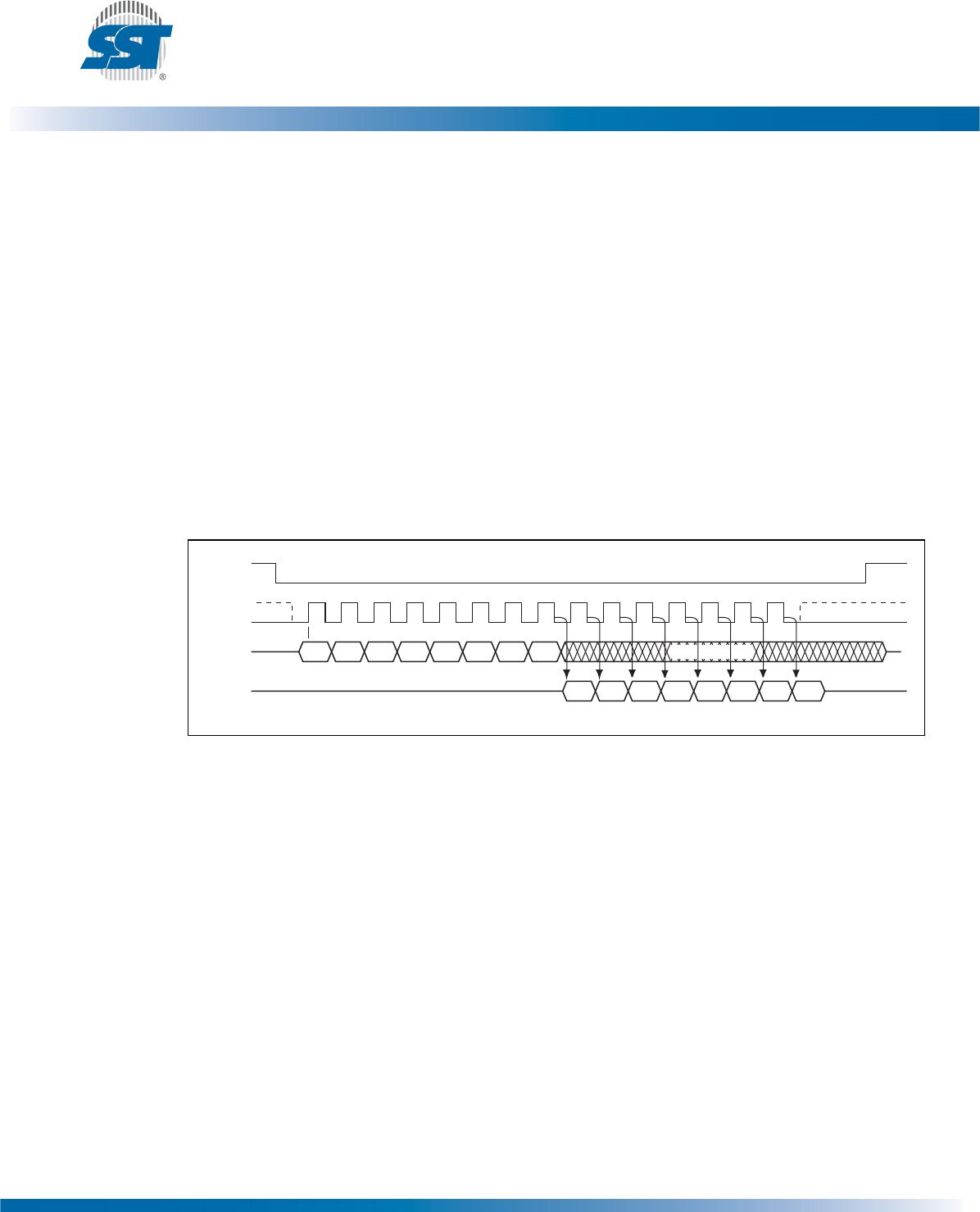
Hold Operation
HOLD# pin is used to pause a serial sequence underway with the SPI flash memory without resetting
the clocking sequence. To activate the HOLD# mode, CE# must be in active low state. The HOLD#
mode begins when the SCK active low state coincides with the falling edge of the HOLD# signal. The
HOLD mode ends when the HOLD# signal’s rising edge coincides with the SCK active low state.
If the falling edge of the HOLD# signal does not coincide with the SCK active low state, then the device
enters Hold mode when the SCK next reaches the active low state. Similarly, if the rising edge of the
HOLD# signal does not coincide with the SCK active low state, then the device exits in Hold mode
when the SCK next reaches the active low state. See Figure 4 for Hold Condition waveform.
Once the device enters Hold mode, SO will be in high-impedance state while SI and SCK can be V
IL
or
V
IH
.
If CE# is driven active high during a Hold condition, it resets the internal logic of the device. As long as
HOLD# signal is low, the memory remains in the Hold condition. To resume communication with the
device, HOLD# must be driven active high, and CE# must be driven active low. See Figure 19 for Hold
timing.
Figure 4: Hold Condition Waveform
Write Protection
SST25LF020A provides software Write protection. The Write Protect pin (WP#) enables or disables
the lock-down function of the status register. The Block-Protection bits (BP1, BP0, and BPL) in the sta-
tus register provide Write protection to the memory array and the status register. See Table 4 for Block-
Protection description.
Active Hold Active Hold Active
1242 F03.0
SCK
HOLD#