Table 5: Thermal Characteristics
Notes 1–3 apply to entire table
Parameter Symbol Value Units Notes
Operating temperature T
C
0 to 85 °C
0 to 95 °C 4
Notes:
1. MAX operating case temperature T
C
is measured in the center of the package, as shown
below.
2. A thermal solution must be designed to ensure that the device does not exceed the
maximum T
C
during operation.
3. Device functionality is not guaranteed if the device exceeds maximum T
C
during
operation.
4. If T
C
exceeds 85°C, the DRAM must be refreshed externally at 2x refresh, which is a 3.9µs
interval refresh rate. The use of self refresh temperature (SRT) or automatic self refresh
(ASR), if available, must be enabled.
Figure 4: Temperature Test Point Location
Test point
Length (L)
Width (W)
0.5 (W)
0.5 (L)
Table 6: Thermal Impedance
Package Substrate
Θ JA (°C/W)
Airflow =
0m/s
Θ JA (°C/W)
Airflow =
1m/s
Θ JA (°C/W)
Airflow =
2m/s Θ JB (°C/W) Θ JC (°C/W) Notes
78-ball Rev A "FSE" Low
conductivity
47.9 36.2 32.0 NA 1.6 1
High
conductivity
28.3 23.0 21.3 10.6 NA
78-ball Rev B "NRE" Low
conductivity
53.5 41.5 37.0 NA 1.5 1
High
conductivity
33.2 27.4 25.6 20.2 NA
Note:
1. Thermal resistance data is based on a number of samples from multiple lots and should
be viewed as a typical number.
16Gb: x4, x8 TwinDie DDR4 SDRAM
Electrical Specifications – Leakages
PDF: 09005aef85fd40a1
DDR4_16Gb_x4_x8_2CS_TwinDie.pdf - Rev. D 12/16 EN
10
Micron Technology, Inc. reserves the right to change products or specifications without notice.
© 2015 Micron Technology, Inc. All rights reserved.
Figure 5: Thermal Impedance
53.5
41.5
37.0
1.5
33.2
27.4
25.6
20.2
0
10
20
30
40
50
60
θJA (0 m/s) θJA (1 m/s) θJA (2 m/s) θJB θJC
Thermal Impedance (°C/W)
Low conductivity test board
High conductivity test board
Note:
1. All simulations are conducted per JEDEC standards.
16Gb: x4, x8 TwinDie DDR4 SDRAM
Electrical Specifications – Leakages
PDF: 09005aef85fd40a1
DDR4_16Gb_x4_x8_2CS_TwinDie.pdf - Rev. D 12/16 EN
11
Micron Technology, Inc. reserves the right to change products or specifications without notice.
© 2015 Micron Technology, Inc. All rights reserved.
Electrical Characteristics – AC and DC Output Measurement Levels
Single-Ended Outputs
Table 7: Single-Ended Output Levels
Parameter Symbol DDR4-1600 to DDR4-3200 Unit
DC output high measurement level (for IV curve linearity) V
OH(DC)
1.1 × V
DDQ
V
DC output mid measurement level (for IV curve linearity) V
OM(DC)
0.8 × V
DDQ
V
DC output low measurement level (for IV curve linearity) V
OL(DC)
0.5 × V
DDQ
V
AC output high measurement level (for output slew rate) V
OH(AC)
(0.7 + 0.15) × V
DDQ
V
AC output low measurement level (for output slew rate) V
OL(AC)
(0.7 - 0.15) × V
DDQ
V
Note:
1. The swing of ±0.15 × V
DDQ
is based on approximately 50% of the static single-ended
output peak-to-peak swing with a driver impedance of RZQ/7 and an effective test load
of 50Ω to V
TT
= V
DDQ
.
Using the same reference load used for timing measurements, output slew rate for fall-
ing and rising edges is defined and measured between V
OL(AC)
and V
OH(AC)
for single-
ended signals.
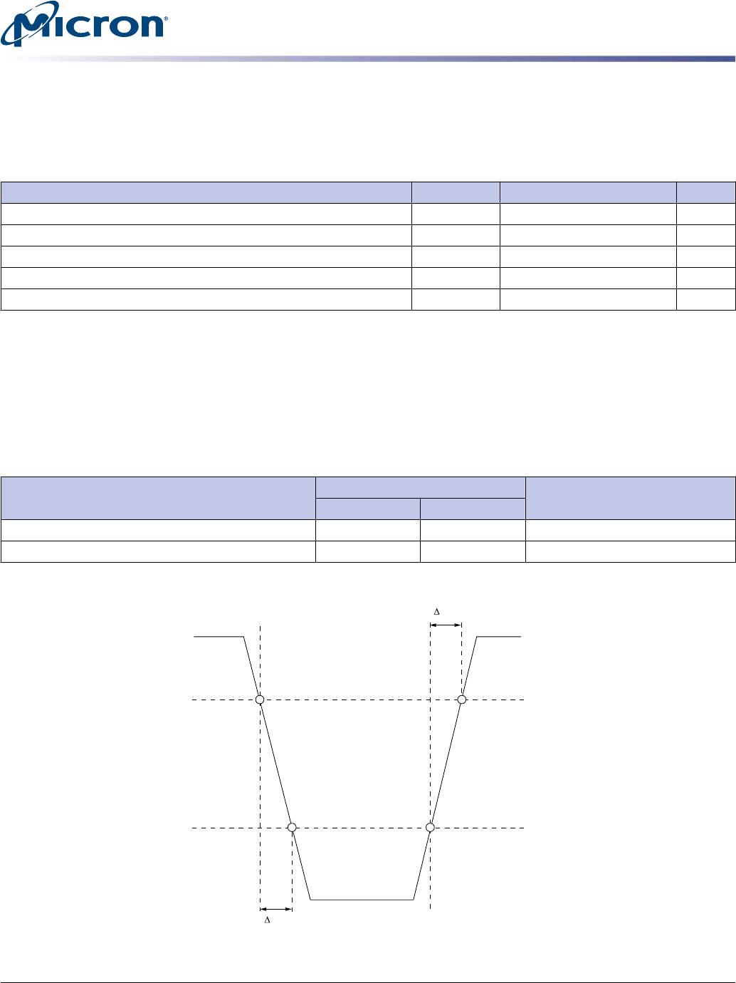
Table 8: Single-Ended Output Slew Rate Definition
Description
Measured
Defined byFrom To
Single-ended output slew rate for rising edge V
OL(AC)
V
OH(AC)
[V
OH(AC)
- V
OL(AC)
]/ΔTR
se
Single-ended output slew rate for falling edge V
OH(AC)
V
OL(AC)
[V
OH(AC)
- V
OL(AC)
]/ΔTF
se
Figure 6: Single-ended Output Slew Rate Definition
TR
se
TF
se
V
OH(AC)
V
OL(AC)
Single-Ended Output Voltage (DQ)
16Gb: x4, x8 TwinDie DDR4 SDRAM
Electrical Characteristics – AC and DC Output Measurement
Levels
PDF: 09005aef85fd40a1
DDR4_16Gb_x4_x8_2CS_TwinDie.pdf - Rev. D 12/16 EN
12
Micron Technology, Inc. reserves the right to change products or specifications without notice.
© 2015 Micron Technology, Inc. All rights reserved.

MT40A2G8FSE-083E:A TR

Mfr. #:
Manufacturer:
Micron
Description:
DRAM DDR4 16G 2GX8 FBGA DDP
Lifecycle:
New from this manufacturer.
Delivery:
DHL FedEx Ups TNT EMS
Payment:
T/T Paypal Visa MoneyGram Western Union