LTC4371
1
4371f
For more information www.linear.com/LTC4371
Typical applicaTion
FeaTures DescripTion
Dual Negative Voltage
Ideal Diode-OR Controller
and Monitor
The LT C
®
4371 is a two-input negative voltage ideal diode-OR
controller that drives external N-channel MOSFETs as a low
dissipation alternative to Schottky diodes in high power 48V
systems. Low power dissipation and voltage loss eliminates
the need for heatsinks and reduces PC board area. Power
sources can be easily ORed together to increase total system
power and reliability.
The LTC4371 tolerates ±300V transients such as those
experienced during lightning-induced surges and input
supply short-circuit events. The internal shunt regulator
and low 350μA quiescent current allow the use of a large
value dropping resistor to protect the supply pin against
high voltage transients, while the high impedance drain
pins can be similarly protected by high value series resis
-
tors without compromising diode operation.
The 220ns
reverse current turn-off is achieved by a power
ful
2A gate driver with low propagation delay, thereby minimizing
peak reverse current under catastrophic fault conditions. Open
MOSFET and fuse faults are indicated at the FAULTB pin, which
is capable of sinking 5mA to drive an LED or opto isolator.
applicaTions
n
Controls N-Channel MOSFETs to Replace Power
Schottky Diodes
n
Low 15mV Forward Voltage Minimizes Dissipation
n
Withstands > ±300V Transients
n
Fast Turn-Off: <220ns
n
Shunt Regulated for High Voltage Applications
n
4.5V Minimum Operation
n
Low 350μA Quiescent Current
n
5mA Gate Pull-Up for 60Hz Applications
n
High Impedance Drain Pins: <10μA Leakage
n
Open Fuse and MOSFET Monitor
n
10-Pin (3mm × 3mm) DFN and MSOP Packages
n
–48V Telecom Power
n
AdvancedTCA Systems
n
Network Routers and Switches
n
Computer Systems and Servers
L, LT, LTC, LTM, Linear Technology and the Linear logo are registered trademarks of Linear
Technology Corporation. All other trademarks are the property of their respective owners.
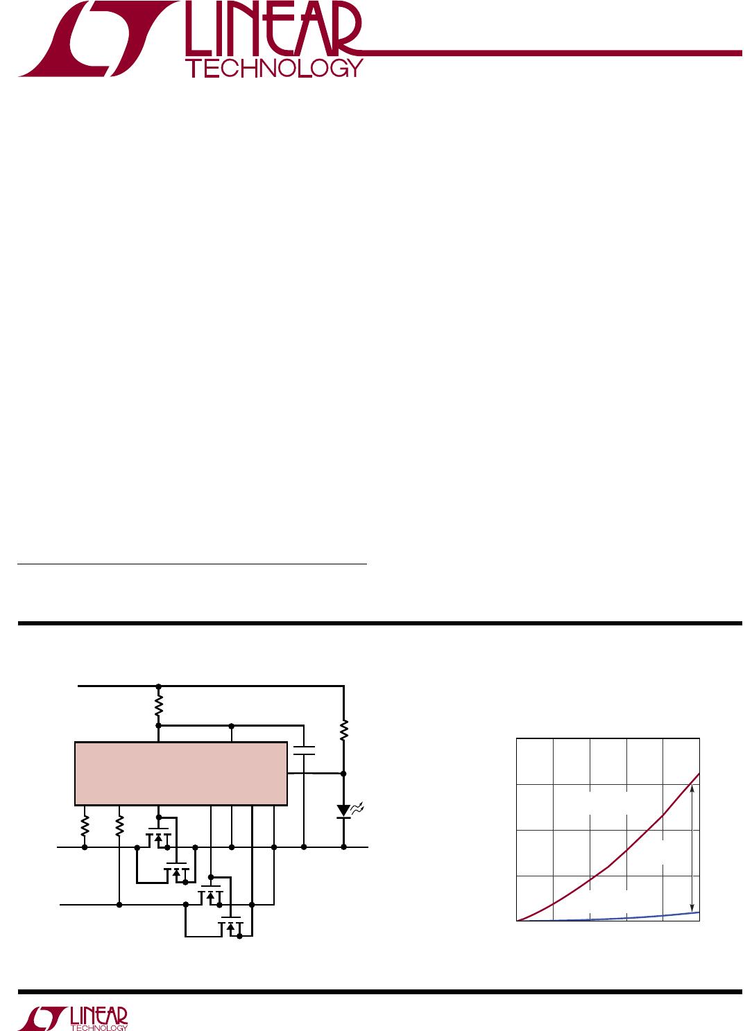
–48V/50A Diode-OR
Power Dissipation vs. Load Current
4371 TA01a
LTC4371
DA DB GBGA SA
V
Z
V
DD
SB V
SS
FAULTB
C1
2.2μF
R
DA
20k
R
DB
20k
M1*
M3*
M2*
V
A
–36V TO
–72V
V
B
–36V TO
–72V
V
OUT
50A LOAD
D1
GREEN LED =
MOSFETS GOOD
R
Z
30k
R1
33k
RTN
M4*
*M1-M4: IPT020N10N3
MOSFET
(2–IPT020N10N3)
SCHOTTKY DIODE
(SBRT60U100CT)
POWER
SAVED
CURRENT (A)
0
0
POWER DISSIPATION (W)
vs Load Current
4371 TA01b
LTC4371
2
4371f
For more information www.linear.com/LTC4371
TOP VIEW
DD PACKAGE
10-LEAD (3mm ×
3mm) PLASTIC DFN
10
11
9
6
7
8
4
5
3
2
1
DB
GB
SB
FAULTB
V
SS
DA
GA
SA
V
Z
V
DD
T
JMAX
= 125°C, θ
JA
= 43°C/W (NOTE 4)
EXPOSED PAD (PIN 11) PCB V
SS
CONNECTION OPTIONAL
1
2
3
4
5
DA
GA
SA
V
Z
V
DD
10
9
8
7
6
DB
GB
SB
FAULTB
V
SS
TOP VIEW
MS PACKAGE
10-LEAD PLASTIC MSOP
T
JMAX
= 125°C, θ
JA
= 160°C/W
pin conFiguraTion
absoluTe MaxiMuM raTings
Supply Voltage V
DD
.................................... 0.3V to 17V
Input Voltage
DA, DB (Note 3) .................................... 40V to 100V
SA, SB .................................................. 0.3V to 0.3V
DC Currents
V
Z
......................................................................20mA
DA, DB ............................................................... ±1mA
Single Pulse Current (6ms) DA, DB ........................10mA
(Notes 1, 2)
orDer inForMaTion
Output Voltages
GA, GB ................................................... 0.3V to V
DD
FAULTB .................................................. 0.3V to 17V
Operating Ambient Temperature Range
LTC4371C ................................................ 0°C to 70°C
LTC4371I .............................................40°C to 85°C
Storage Temperature Range .................. 65°C to 150°C
Lead Temperature (Soldering, 10 sec)
MS Package ......................................................300°C
LEAD FREE FINISH TAPE AND REEL PART MARKING PACKAGE DESCRIPTION TEMPERATURE RANGE
LTC4371CDD#PBF LTC4371CDD#TRPBF LGSD 10-Lead (3mm × 3mm) Plastic DFN 0°C to 70°C
LTC4371IDD#PBF LTC4371IDD#TRPBF LGSD 10-Lead (3mm × 3mm) Plastic DFN –40°C to 85°C
LTC4371CMS#PBF LTC4371CMS#TRPBF LTGSF 10-Lead Plastic MSOP 0°C to 70°C
LTC4371IMS#PBF LTC4371IMS#TRPBF LTGSF 10-Lead Plastic MSOP –40°C to 85°C
Consult LTC Marketing for parts specified with wider operating temperature ranges.
For more information on lead free part marking, go to: http://www.linear.com/leadfree/
For more information on tape and reel specifications, go to: http://www.linear.com/tapeandreel/. Some packages are available in 500 unit reels through
designated sales channels with #TRMPBF suffix.
(http://www.linear.com/product/LTC4371#orderinfo)
LTC4371
3
4371f
For more information www.linear.com/LTC4371
elecTrical characTerisTics
The l denotes the specifications which apply over the full operating
temperature range, otherwise specifications are at T
A
= 25°C, I
Z
= 50µA, V
DD
= 12.4V, SA = SB = V
SS
unless otherwise noted.
SYMBOL PARAMETER CONDITIONS MIN TYP MAX UNITS
V
DD
Input Supply Range
l
4.5 16 V
I
DD
Input Supply Current
Normal Operation
Gate Fault to V
SS ,
Strong Pull-Up Disabled
Gate Fault to V
SS,
Strong Pull-Up Enabled
∆V
SD
= ±0.1V
V
Z
= 10.4V, ∆V
SD
= 0.1V, One GATE = V
SS
I
Z
= 50µA, ∆V
SD
= 0.1V, One GATE = V
SS
l
l
l
200
400
4.5
300
550
7
450
750
9.5
µA
µA
mA
V
Z
Shunt Regulator Voltage I
Z
= 50µA
l
11.8 12.4 14 V
∆V
Z
Shunt Regulator Load Regulation I
Z
= 50µA to 10mA
l
600 mV
V
Z(PU)
V
Z
High Threshold to Enable Strong Gate Pull-Up V
DD
= V
Z
Rising
l
10.7 11.2 11.8 V
∆V
Z(PU)
V
Z
High Threshold Hysteresis 0.5 V
V
Z(PU)
V
Z
Low Threshold to Enable Strong Gate Pull-Up V
Z
Falling
l
1.15 1.25 1.35 V
∆V
SD
Source-Drain Forward Servo Voltage
l
5 15 25 mV
∆V
GATE
Gate Drive (V
G
– V
S
) I
G
= 0µA, –1µA; ∆V
SD
= 100mV
l
V
DD
– 0.2 V
DD
+ 0.1 V
I
GATE(UP)
Gate Pull-Up Current ∆V
SD
= 100mV, ∆V
GATE
= 5V
l
–3 –5 –8 mA
I
GATE(DN)
Gate Pull-Down Current
Strong Gate Pull-Down Current
∆V
SD
= –10mV, ∆V
GATE
= 5V
∆V
SD
= –100mV, ∆V
GATE
= 5V
l
l
7
1
10
2
13
3
mA
A
t
OFF
Gate Turn-Off Time in Fault Condition ∆V
SD
= 0.1V Step to –0.4V,
C
GATE
= 3.3nF, ∆V
GATE
<1V
l
220 ns
I
D
DA, DB Leakage Current
MOSFET Off
MOSFET Open
V
D
= 80V
V
D
= –40V
l
l
10
–10
µA
µA
R
D
DA, DB Resistance ∆V
SD
= –50mV to 0.1V
l
1 2 5
V
BVD
DA, DB Breakdown Voltage I
D
= 10mA, 6ms
l
100 130 170 V
I
S
SA, SB Leakage Current V
S
= 0V
l
±2 μA
∆V
SD(FLT)
Source-Drain Fault Detection Threshold
l
150 200 225 mV
V
FAULTB
FAULTB Output Low I
FAULTB
= 5mA
l
0.4 V
I
FAULTB
FAULTB Leakage Current V
FAULTB
= 16V
l
±1 μA
Note 1: Stresses beyond those listed under Absolute Maximum Ratings
may cause permanent damage to the device. Exposure to any Absolute
Maximum Rating condition for extended periods may affect device
reliability and lifetime.
Note 2: All currents into pins are positive; all voltages are referenced to
V
SS
unless otherwise specified.
Note 3: An internal clamp limits the DA and DB pins to a minimum of
100V above V
SS
and –40V below V
SS
. This pin can be safely tied to higher
voltages through a resistance that limits the current below 1mA DC or
10mA for a 6ms transient. Driving this pin with current beyond the clamp
may damage the device.
Note 4: Thermal resistance is specified with exposed pad soldered to a
3-inch by 4.5-inch, four layer FR4 board. If exposed pad is not soldered
θ
JA
= 93°C/ W.

LTC4371CMS#TRPBF

Mfr. #:
Manufacturer:
Analog Devices Inc.
Description:
Power Management Specialized - PMIC 2x Neg V Ideal Diode-OR Cntr & Mon
Lifecycle:
New from this manufacturer.
Delivery:
DHL FedEx Ups TNT EMS
Payment:
T/T Paypal Visa MoneyGram Western Union