LTC4371
13
4371f
For more information www.linear.com/LTC4371
applicaTions inForMaTion
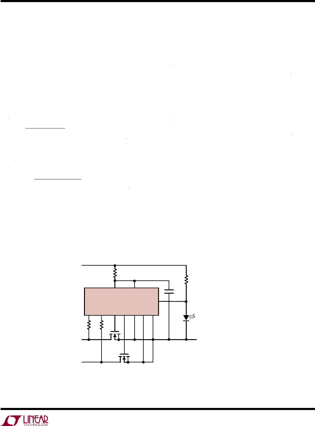
Figure 11. Fuse and Open MOSFET Detection
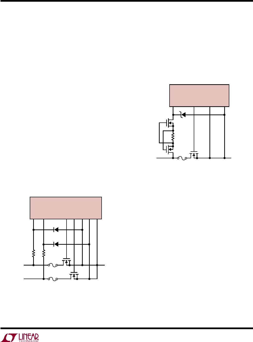
Figure 12. Back-to-Back Drain Pin Limiter for ±600V
Fuse and Open MOSFET Detection
The LTC4371 monitors ∆V
SD
of each channel as measured
across SA DA and SB DB. If ∆V
SD
of either channel
exceeds 200mV and the associated gate pin is driven fully
on, FAULTB pulls low to indicate a fault. Conditions lead
-
ing to high ∆V
SD
include excessive load current (I
LOAD
×
R
DS(ON)
> 200mV), an open circuit MOSFET or an open
fuse placed in series with the MOSFET. A high ∆V
SD
fault
is detected on only the highest voltage input supply, i.e.
the path that should be supplying power is, as a result of
one of the aforementioned conditions, unable to do so.
Temporary conditions, such as the initial 700mV drop
experienced when an input first rises to the point of sup
-
plying current but before the gate has been driven on, are
masked since the gate must also be high for fault detection.
The ∆V
SD
monitor can be used to detect open fuses, as
shown in Figure11. An open fuse gives the same signa-
ture as an open MOSFET:
V
SD
increases beyond 200mV
when the affected input surpasses the opposing channel.
The connection shown in Figure 11 introduces a new
problem: an open fuse and open MOSFET exposes the DA
and DB pins to high negative voltage with respect to V
SS
.
Diodes D1 and D2 clamp the DA, DB pins from exceeding
the absolute maximum of –40V with respect to V
SS
.
Figure12 shows a protection method that extends DA and
DB pin operation to ±600V. The drain pins are clamped
by an 82V Zener diode. As shown, the DA pin is clamped
at 82V with respect to V
SS
in the positive direction, and
700mV below V
SS
in the negative direction. When a high
input voltage of either polarity is present, back-to-back
depletion mode N-channel MOSFETs limit the current in
the Zener diode to V
GS(TH)
/R
DA
(100μA for R
DA
= 20kΩ),
a value that is indefinitely sustainable.
FAULTB Pin
The open drain FAULTB pin pulls low when the ∆V
SD
of
either channel exceeds 200mV, while its gate is driven
fully on. FAULTB can sink 5mA to drive an LED for visual
indication, or an opto isolator to communicate across an
isolation barrier. The FAULTB pin voltage is limited to 17V
absolute maximum with respect to V
SS
in the high state
and cannot be pulled up to return except in low voltage
applications.
In Figure13, the FAULTB pin is used to shunt current away
from a green LED; the LED indicates (illuminates when) no
fault condition is present. The operating voltage is limited
at the low end by the minimum acceptable LED current,
and at the high end by the FAULTB pin’s 5mA capability.
Figure14 shows a simple implementation driving a red
LED; the LED indicates a fault condition is present. While
this simple configuration works well in –48V applications,
the maximum operating voltage is limited to 100V, the LED
4371 F11
LTC4371
DA DB GA GB SA SB V
SS
R
DA
20k
R
DB
20k
M1
M2
V
A
–36V TO
–72V
V
B
–36V TO
–72V
V
OUT
D1
1N4148W
D2
1N4148W
F1
F2
4371 F12
LTC4371
DA GA SA V
SS
M2*
M3*
M1
V
A
V
OUT
R
DA
20k
82V
*M2, M3: BSP135 (600V) DEPLETION NMOS
LTC4371
14
4371f
For more information www.linear.com/LTC4371
applicaTions inForMaTion
Figure 13. FAULTB Drives a Green LED in Shunt Mode
Figure 14. FAULTB Drives a Red LED in Series Mode
Figure 15. FAULTB Driving an LED in a High Voltage Application
Figure 16. Recommended PCB Layout for M1, M2 and C1
C1
V
OUT
V
B
V
A
R
DB
R
DA
4371 F16
M1
M2
LTC4371
4371 F13
LTC4371
V
SS
V
OUT
D1
GREEN LED = MOSFETS GOOD
R1
33k
RTN
FAULTB
4371 F14
LTC4371
V
SS
V
OUT
D1
RED LED = MOSFET BAD
R1
20k
500mW
R2
3.9k
RTN
FAULTB
4371 F15
LTC4371
V
SS
V
DD
V
OUT
–600V MAX
D1
RED LED = MOSFET BAD
R2
10k
M2
BSP125
RTN
FAULTB
current varies widely with operating voltage, and dissipation
in the 20kΩ resistor reaches ≈250mW at 72V input. These
shortcomings are eliminated by the slightly more complex
circuit shown in Figure15. A cascode shields the FAULTB
pin from the high input voltage and dissipates no power
under normal conditions, while the LED current remains
constant regardless of input voltage when indicating a fault.
At 600V, cascode dissipation reaches 600mW maximum.
Layout Considerations
A sample layout for the LTC4371 DFN package and PG-
HSOF-8 MOSFET package is shown in Figure16.
The V
DD
bypass capacitor C1 provides AC current to the
device; place it as close to V
DD
and V
SS
pins as possible.
Connect the gate amplifier input pins, DA, DB, SA and SB,
directly to the MOSFETs drain and source terminals using
Kelvin connections for good accuracy. Place the MOSFET
sources as close together as possible, with V
SS
connecting
at their intersection.
Keep the traces to the MOSFET drains and common source
wide and short. A good rule-of-thumb for minimizing
self-heating effects in the copper traces is to allow at least
1-inch trace width per 50 amperes, for a surface layer of
1-ounce copper. This current density corresponds to a self-
heating effect of about 1.3W per square inch. The traces
associated with the power path through the MOSFETs must
have low resistance to maintain good efficiency and low
drop. The resistance of 1-ounce copper is approximately
500μΩ per square.
LTC4371
15
4371f
For more information www.linear.com/LTC4371
applicaTions inForMaTion
Figure 17. –36V to –72V/25A Ideal Diode-OR
4371 F17
LTC4371
DA DB GA GB SA
V
Z
V
DD
SB V
SS
C1
2.2μF
R
DA
20k
R
DB
20k
M1
IPT020N10N3
M2
IPT020N10N3
V
A
–36V TO
–72V
V
B
–36V TO
–72V
V
OUT
25A LOAD
D1
GREEN LED = MOSFETS GOOD
R
Z
30k
R1
33k
RTN
FAULTB
Design Example
The following design example demonstrates the calcula-
tions involved for selecting external components. Consider
a –
48V
application with a –36V to –72V operating range,
200V peak transient and 25A maximum load current (see
Figure17).
The simplest configuration is chosen to power V
DD
, since
this arrangement easily handles the operating conditions
found in a –48V telecom power system. The bias resistor,
R
Z
, is calculated from Equation 1:
R
Z
<
36V 11.8V
750µA
= 32.2kΩ (9)
The nearest lower 5% value is 30kΩ.
The worst case power dissipation in R
Z
:
P
D(RZ)
=
(72V 11.8V)
2
30k
= 166mW (10)
A 30kΩ 0.25W resistor is selected for R
Z
. The maximum
V
Z
current is confirmed from Equation 3 as a safe value
of 2mA. A –200V transient pushes this to 6.3mA, safely
below the maximum allowable V
Z
current of 10mA.
Next, choose the N-channel MOSFET. The 100V,
IPT020N10N3 in a PG-HSOF-8 package with R
DS(ON)
=2mΩ
(max) offers a good solution.
The maximum voltage drop across the MOSFET is:
∆V
SD
=
25A 2mΩ
=
50mV (11)
which is well below the 150mV minimum ∆V
SD
fault
threshold.
From Equation 7, the maximum power dissipation in the
MOSFET is:
P
D(MOSFET)
= 25A
2
2mΩ = 1.25W (12)
a reasonable value for the proposed package.
The minimum recommended value of 20kΩ is chosen for
R
DA
and R
DB
. 20kΩ protects the DA and DB pins to 300V.
The LED, D1, requires at least 1mA of current to turn on
fully; therefore, R1 is set to 33k to accommodate the mini
-
mum input supply voltage of –36V. The maximum current
is 2mA at –72V, but excursions to 200V give 6mA, slightly
beyond the FAULTB pin’s 5mA capability. This means that
if there is a fault present, a brief glitch might cause a “no
fault” indication during a 200V transient. Since D1 is a
visual indicator, well accept the remote chance of a dim
flash in exchange for the simple circuit solution.

LTC4371CMS#TRPBF

Mfr. #:
Manufacturer:
Analog Devices Inc.
Description:
Power Management Specialized - PMIC 2x Neg V Ideal Diode-OR Cntr & Mon
Lifecycle:
New from this manufacturer.
Delivery:
DHL FedEx Ups TNT EMS
Payment:
T/T Paypal Visa MoneyGram Western Union