LTC4371
19
4371f
For more information www.linear.com/LTC4371
Typical applicaTions
4371 F23
+
48V
CT
LTC4371
DA DB GA GB SA
V
Z
V
DD
SB V
SS
FAULTB
C1
2.2μF
R
DA
20k
R
DB
20k
M1
IPT020N10N3
M2
IPT020N10N3
V
A
V
B
+
D1
GREEN LED
= MOSFETS GOOD
R
Z
10k
R1
22k
CL
4×1000μF
SUNCON ME-WX
24VDC
4A
117VAC
Figure23. Full Wave Center Tap Rectifier
LTC4371
20
4371f
For more information www.linear.com/LTC4371
package DescripTion
Please refer to http://www.linear.com/product/4371#packaging for the most recent package drawings.
MSOP (MS) 0213 REV F
0.53 ±0.152
(.021 ±.006)
SEATING
PLANE
0.18
(.007)
1.10
(.043)
MAX
0.17 –0.27
(.007 – .011)
TYP
0.86
(.034)
REF
0.50
(.0197)
BSC
1 2
3
4 5
4.90 ±0.152
(.193 ±.006)
0.497 ±0.076
(.0196 ±.003)
REF
8910
7
6
3.00 ±0.102
(.118 ±.004)
(NOTE 3)
3.00 ±0.102
(.118 ±.004)
(NOTE 4)
NOTE:
1. DIMENSIONS IN MILLIMETER/(INCH)
2. DRAWING NOT TO SCALE
3. DIMENSION DOES NOT INCLUDE MOLD FLASH, PROTRUSIONS OR GATE BURRS.
MOLD FLASH, PROTRUSIONS OR GATE BURRS SHALL NOT EXCEED 0.152mm (.006") PER SIDE
4. DIMENSION DOES NOT INCLUDE INTERLEAD FLASH OR PROTRUSIONS.
INTERLEAD FLASH OR PROTRUSIONS SHALL NOT EXCEED 0.152mm (.006") PER SIDE
5. LEAD COPLANARITY (BOTTOM OF LEADS AFTER FORMING) SHALL BE 0.102mm (.004") MAX
0.254
(.010)
0° – 6° TYP
DETAIL “A”
DETAIL “A”
GAUGE PLANE
5.10
(.201)
MIN
3.20 – 3.45
(.126 – .136)
0.889 ±0.127
(.035 ±.005)
RECOMMENDED SOLDER PAD LAYOUT
0.305 ±0.038
(.0120 ±.0015)
TYP
0.50
(.0197)
BSC
0.1016 ±0.0508
(.004 ±.002)
MS Package
10-Lead Plastic MSOP
(Reference LTC DWG # 05-08-1661 Rev F)
LTC4371
21
4371f
For more information www.linear.com/LTC4371
Information furnished by Linear Technology Corporation is believed to be accurate and reliable.
However, no responsibility is assumed for its use. Linear Technology Corporation makes no representa-
tion that the interconnection of its circuits as described herein will not infringe on existing patent rights.
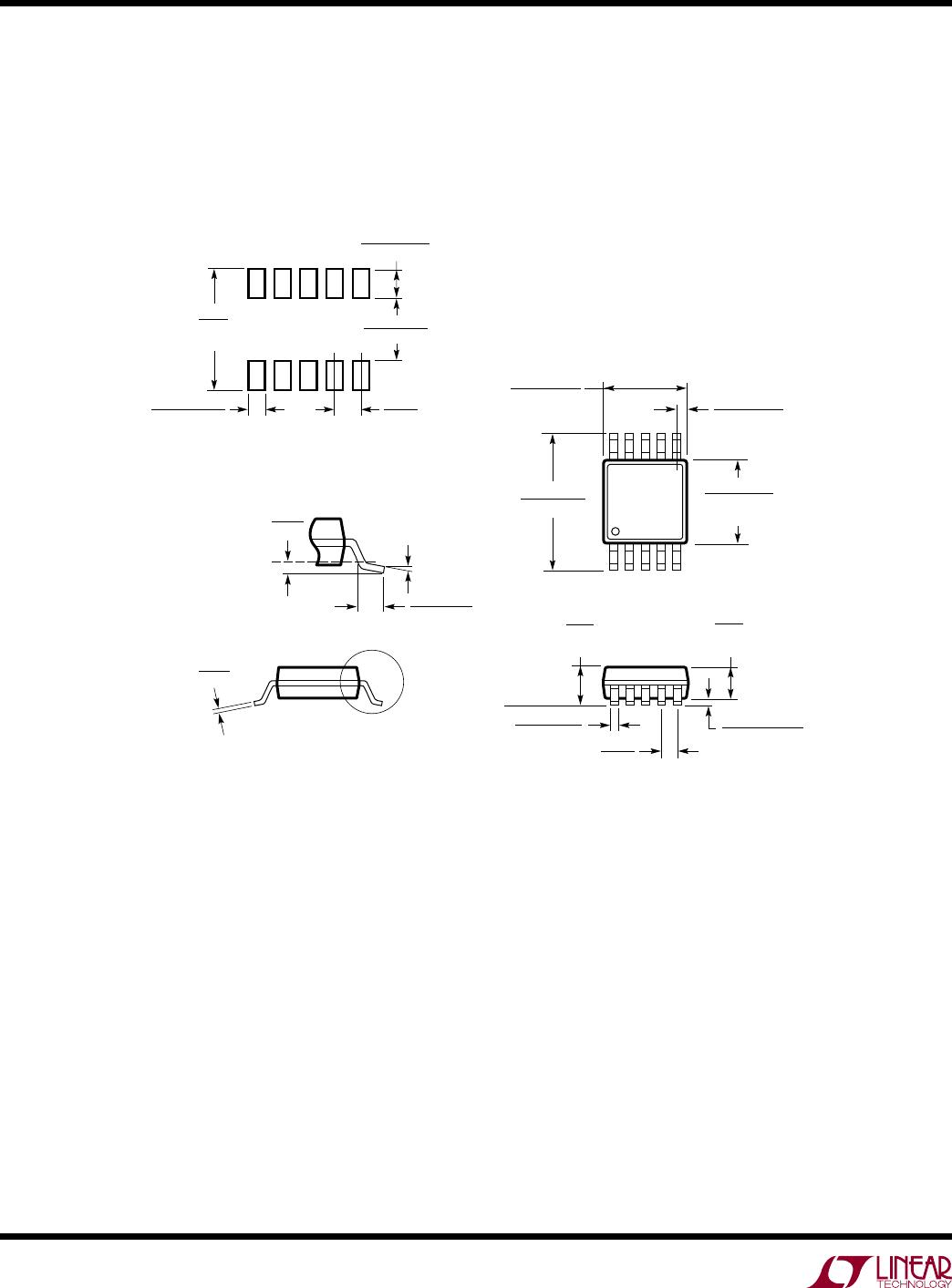
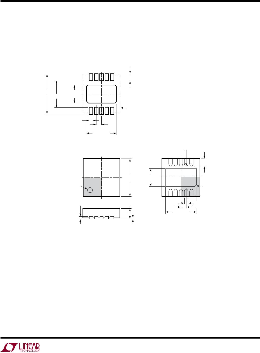
package DescripTion
Please refer to http://www.linear.com/product/4371#packaging for the most recent package drawings.
3.00 ±0.10
(4 SIDES)
NOTE:
1. DRAWING TO BE MADE A JEDEC PACKAGE OUTLINE M0-229 VARIATION OF (WEED-2).
CHECK THE LTC WEBSITE DATA SHEET FOR CURRENT STATUS OF VARIATION ASSIGNMENT
2. DRAWING NOT TO SCALE
3. ALL DIMENSIONS ARE IN MILLIMETERS
4. DIMENSIONS OF EXPOSED PAD ON BOTTOM OF PACKAGE DO NOT INCLUDE
MOLD FLASH. MOLD FLASH, IF PRESENT, SHALL NOT EXCEED 0.15mm ON ANY SIDE
5. EXPOSED PAD SHALL BE SOLDER PLATED
6. SHADED AREA IS ONLY A REFERENCE FOR PIN 1 LOCATION ON THE
TOP AND BOTTOM OF PACKAGE
0.40 ±0.10
BOTTOM VIEW—EXPOSED PAD
1.65 ±0.10
(2 SIDES)
0.75 ±0.05
R = 0.125
TYP
2.38 ±0.10
(2 SIDES)
15
106
PIN 1
TOP MARK
(SEE NOTE 6)
0.200 REF
0.00 – 0.05
(DD) DFN REV C 0310
0.25 ±0.05
2.38 ±0.05
(2 SIDES)
RECOMMENDED SOLDER PAD PITCH AND DIMENSIONS
1.65 ±0.05
(2 SIDES)2.15 ±0.05
0.50
BSC
0.70 ±0.05
3.55 ±0.05
PACKAGE
OUTLINE
0.25 ±0.05
0.50 BSC
DD Package
10-Lead Plastic DFN (3mm × 3mm)
(Reference LTC DWG # 05-08-1699 Rev C)
PIN 1 NOTCH
R = 0.20 OR
0.35 × 45°
CHAMFER

LTC4371CMS#TRPBF

Mfr. #:
Manufacturer:
Analog Devices Inc.
Description:
Power Management Specialized - PMIC 2x Neg V Ideal Diode-OR Cntr & Mon
Lifecycle:
New from this manufacturer.
Delivery:
DHL FedEx Ups TNT EMS
Payment:
T/T Paypal Visa MoneyGram Western Union