LTC4371
7
4371f
For more information www.linear.com/LTC4371
operaTion
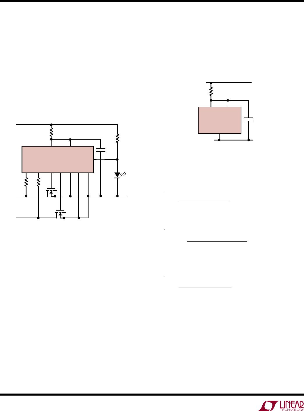
The LTC4371 controls N-channel MOSFETs to emulate two
ideal diodes (see Block Diagram). By sensing the MOSFET’s
source-to-drain voltage drop, amplifiers AMPA and AMPB
control the gate of their respective external MOSFET to act
as an ideal diode with a 15mV forward (∆V
SD
) drop. With
low load currents, the amplifier regulates the MOSFET gate
near its threshold to maintain a forward drop of 15mV. As
load current increases, the gate voltage is driven higher
to maintain a drop of 15mV. For very large load currents
where the MOSFET gate is driven fully on, the forward drop
rises linearly with current according to R
DS(ON)
• I
LOAD
. If
the forward drop is less than 15mV, or if ∆V
SD
reverses,
the amplifier turns the MOSFET off and the load current
transfers to the other channel.
When the power supply voltages are nearly equal, this
regulation technique ensures that the load current is
smoothly shared between the supplies without oscilla
-
tion. The current balance depends on the R
DS(ON)
of the
MOSFETs and the output resistance of the supplies.
In the case of supply failure, such as supply V
A
, while
conducting most or all of the load current is shorted to
return, a large reverse current flows from return through
M1 to any load capacitance and through M2 to supplyV
B
.
AMPA detects the current reversal and turns off M1 in less
than 220ns. Fast turn-off prevents reverse current from
rising to a damaging level.
The remaining supply V
B
delivers load current through
the body diode of M2, until the gate is driven on. With
700mV forward drop across M2, AMPB responds quickly
and drives the gate with 5mA pull-up current, limiting
the body diode conduction time to under 100μs. This
minimizes power dissipation arising from switchover and
is especially important in 60Hz AC applications. As the
forward drop reduces, a weaker output stage takes over
and regulates the forward drop, within the limitations of
R
DS(ON)
, to 15mV.
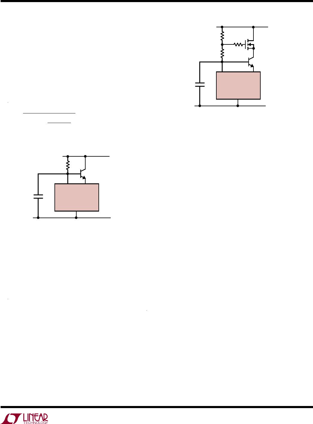
The LTC4371 can be powered in –4.5V to –16V applica-
tions by connecting V
DD
directly to the power supply
return. In higher voltage applications or to guard against
input transients, V
Z
and V
DD
can be connected together
and powered from return through a bias resistor, R
Z
. For
repetitive 5mA gate pull-up current, V
DD
can be driven
by a buffer biased by V
Z
. The V
Z
pin is shunt regulated to
12.4V with respect to V
SS
with 50μA minimum bias, and
is capable of sinking up to 10mA.
The LTC4371 is designed to withstand high voltage tran
-
sients exceeding ±300V, such as those experienced during
lightning-induced surges and input supply short circuit
events, without damage. 130V internal clamps protect
drain pins DA and DB against positive spikes. External
resistors R
DA
and R
DB
are necessary to limit the peak
clamp current to less than 10mA.
In an application circuit, negative spikes are clamped by
the MOSFET’s body diode to V
OUT
, such that the drain
pin never sees more than –700mV with respect to V
SS
. A
safely clamped negative transient on one input manifests
itself as a positive transient on the second input and as
an increased voltage from RTN to V
OUT
. The bias resistor,
R
Z
, limits the current into the V
Z
shunt regulator to less
than 10mA.
A Fault Detection circuit monitors MOSFET ∆V
SD
; FAULTB
pulls low if ∆V
SD
of either channel exceeds 200mV while
the gate is driven fully on. This is an indication of an open
circuit MOSFET and can be configured for fuse monitor
-
ing by moving the drain pin connection to the input side
of the fuse.