Feature Description
Configuration Dedicated Secure Device Manager
Software programmable device configuration
Serial and parallel flash interface
Configuration via protocol (CvP) using PCI Express Gen1/Gen2/Gen3
Fine-grained partial reconfiguration of core fabric
Dynamic reconfiguration of transceivers and PLLs
Comprehensive set of security features including AES-256, SHA-256/384, and
ECDSA-256/384 accelerators, and multi-factor authentication
Physically Unclonable Function (PUF) service
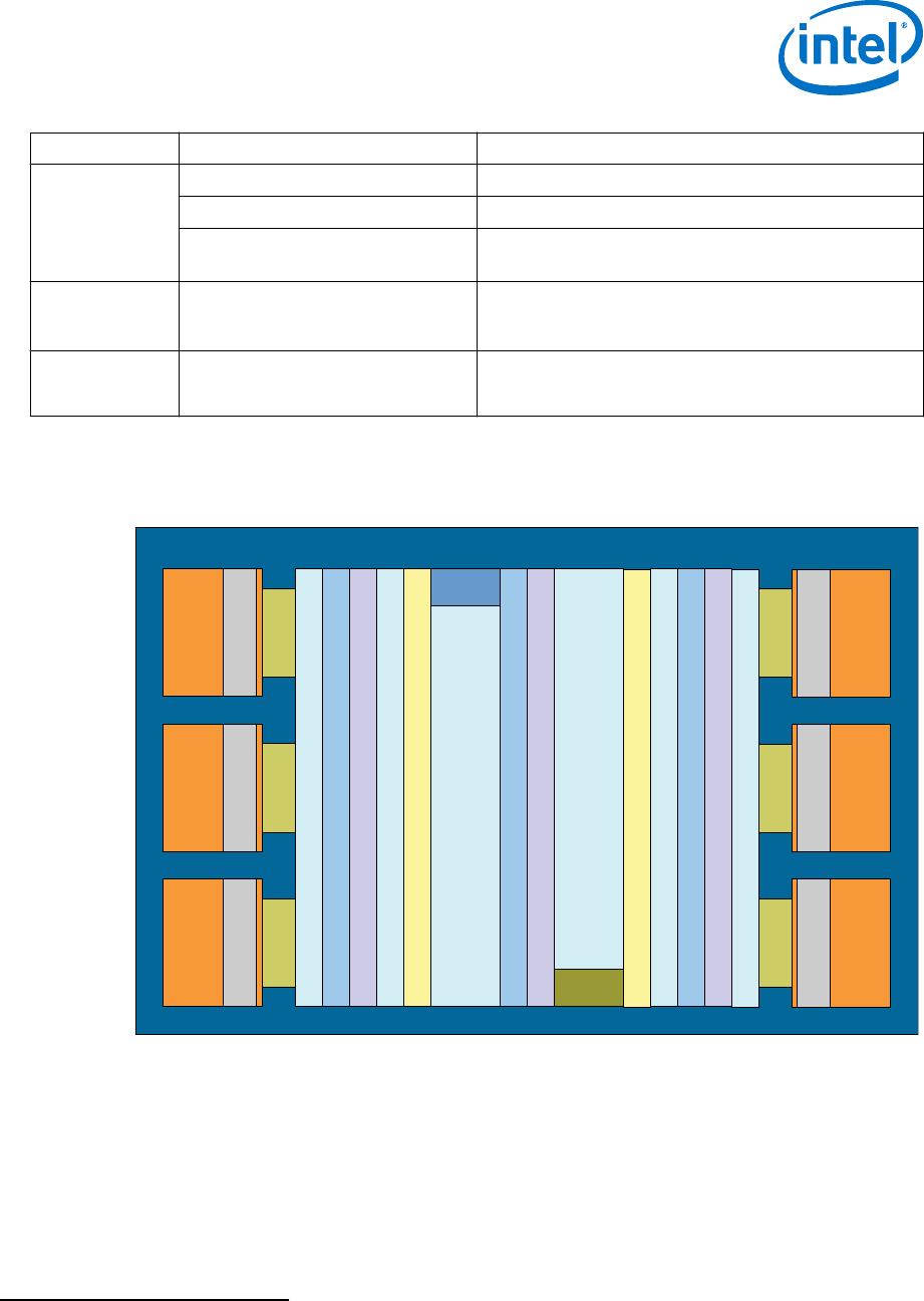
Packaging Intel Embedded Multi-die Interconnect Bridge (EMIB) packaging technology
Multiple devices with identical package footprints allows seamless migration across
different device densities
1.0 mm ball-pitch FBGA packaging
Lead and lead-free package options
Software and tools Intel Quartus Prime Pro Edition design suite with new compiler and Hyper-Aware design
flow
Fast Forward compiler to allow HyperFlex architecture performance exploration
Transceiver toolkit
Platform designer integration tool
DSP Builder advanced blockset
OpenCL
support
SoC Embedded Design Suite (EDS)
Table 3. Intel Stratix 10 SoC Specific Device Features
SoC Subsystem Feature Description
Hard Processor
System
Multi-processor unit (MPU) core Quad-core ARM Cortex-A53 MPCore processor with ARM
CoreSight debug and trace technology
Scalar floating-point unit supporting single and double
precision
ARM NEON media processing engine for each processor
System Controllers System Memory Management Unit (SMMU)
Cache Coherency Unit (CCU)
Layer 1 Cache 32 KB L1 instruction cache with parity
32 KB L1 data cache with ECC
Layer 2 Cache 1 MB Shared L2 Cache with ECC
On-Chip Memory 256 KB On-Chip RAM
Direct memory access (DMA) controller 8-Channel DMA
Ethernet media access controller
(EMAC)
Three 10/100/1000 EMAC with integrated DMA
USB On-The-Go controller (OTG) 2 USB OTG with integrated DMA
UART controller 2 UART 16550 compatible
Serial Peripheral Interface (SPI)
controller
4 SPI
I
2
C controller 5 I
2
C controllers
SD/SDIO/MMC controller 1 eMMC version 4.5 with DMA and CE-ATA support
SD, including eSD, version 3.0
SDIO, including eSDIO, version 3.0
CE-ATA - version 1.1
continued...
1. Intel
®
Stratix
®
10 GX/SX Device Overview
S10-OVERVIEW | 2018.08.08
Stratix 10 GX/SX Device Overview
10
SoC Subsystem Feature Description
NAND flash controller 1 ONFI 1.0, 8- and 16-bit support
General-purpose I/O (GPIO) Maximum of 48 software programmable GPIO
Timers 4 general-purpose timers
4 watchdog timers
Secure Device
Manager
Security Secure boot
Advanced Encryption Standard (AES) and authentication
(SHA/ECDSA)
External
Memory
Interface
External Memory Interface Hard Memory Controller with DDR4 and DDR3, and
LPDDR3
1.4. Intel Stratix 10 Block Diagram
Figure 2. Intel Stratix 10 FPGA and SoC Architecture Block Diagram
Transceiver Tile
(24 Channels)
PCIe Gen3 Hard IP
EMIB
Transceiver Tile
(24 Channels)
PCIe Gen3 Hard IP
EMIB
Transceiver Tile
(24 Channels)
PCIe Gen3 Hard IP
EMIB
Variable-Precision, Hard Floating-Point DSP Blocks
M20K Embedded Memory Blocks
Hard Memory Controllers, I/O PLLs General-Purpose I/O Cells, LVDS
HyperFlex Core Logic Fabric
HPS
Variable-Precision, Hard Floating-Point DSP Blocks
M20K Embedded Memory Blocks
HyperFlex Core Logic Fabric
SDM
Hard Memory Controllers, I/O PLLs General-Purpose I/O Cells, LVDS
Variable-Precision, Hard Floating-Point DSP Blocks
M20K Embedded Memory Blocks
Transceiver Tile
(24 Channels)
PCIe Gen3 Hard IP
EMIB
Transceiver Tile
(24 Channels)
PCIe Gen3 Hard IP
EMIB
Transceiver Tile
(24 Channels)
PCIe Gen3 Hard IP
EMIB
Package Substrate
HPS: Quad ARM Cortex-A53 Hard Processor System
SDM: Secure Device Manager
EMIB: Embedded Multi-Die Interconnect Bridge
HyperFlex Core Logic Fabric
1.5. Intel Stratix 10 FPGA and SoC Family Plan
(1)
The number of 27x27 multipliers is one-half the number of 18x19 multipliers.
1. Intel
®
Stratix
®
10 GX/SX Device Overview
S10-OVERVIEW | 2018.08.08
Stratix 10 GX/SX Device Overview
11
Table 4. Intel Stratix 10 GX/SX FPGA and SoC Family Plan—FPGA Core (part 1)
Intel Stratix 10
GX/SX Device
Name
Logic Elements
(KLE)
M20K Blocks M20K Mbits MLAB Counts MLAB Mbits 18x19 Multi-
pliers
(1)
GX 400/
SX 400
378 1,537 30 3,204 2 1,296
GX 650/
SX 650
612 2,489 49 5,184 3 2,304
GX 850/
SX 850
841 3,477 68 7,124 4 4,032
GX 1100/
SX 1100
1,092 4,401 86 9,540 6 5,040
GX 1650/
SX 1650
1,624 5,851 114 13,764 8 6,290
GX 2100/
SX 2100
2,005 6,501 127 17,316 11 7,488
GX 2500/
SX 2500
2,422 9,963 195 20,529 13 10,022
GX 2800/
SX 2800
2,753 11,721 229 23,796 15 11,520
GX 4500/
SX 4500
4,463 7,033 137 37,821 23 3,960
GX 5500/
SX 5500
5,510 7,033 137 47,700 29 3,960
Table 5. Intel Stratix 10 GX/SX FPGA and SoC Family Plan—Interconnects, PLLs and
Hard IP (part 2)
Intel Stratix 10
GX/SX Device
Name
Interconnects PLLs Hard IP
Maximum GPIOs Maximum XCVR fPLLs I/O PLLs PCIe Hard IP
Blocks
GX 400/
SX 400
392 24 8 8 1
GX 650/
SX 650
400 48 16 8 2
GX 850/
SX 850
736 48 16 15 2
GX 1100/
SX 1100
736 48 16 15 2
GX 1650/
SX 1650
704 96 32 14 4
GX 2100/
SX 2100
704 96 32 14 4
GX 2500/
SX 2500
1160 96 32 24 4
continued...
1. Intel
®
Stratix
®
10 GX/SX Device Overview
S10-OVERVIEW | 2018.08.08
Stratix 10 GX/SX Device Overview
12

1SX250LH3F55I2LG

Mfr. #:
Manufacturer:
Intel / Altera
Description:
FPGA - Field Programmable Gate Array
Lifecycle:
New from this manufacturer.
Delivery:
DHL FedEx Ups TNT EMS
Payment:
T/T Paypal Visa MoneyGram Western Union