Figure 4. HyperFlex Core Architecture
ALM ALM ALM
ALM ALM ALM
ALM ALM ALM
New Hyper-Registers throughout the core fabric
1.7. Heterogeneous 3D SiP Transceiver Tiles
Intel Stratix 10 FPGAs and SoCs feature power efficient, high bandwidth, low latency
transceivers. The transceivers are implemented on heterogeneous 3D System-in-
Package (SiP) transceiver tiles, each containing 24 full-duplex transceiver channels. In
addition to providing a high-performance transceiver solution to meet current
connectivity needs, this allows for future flexibility and scalability as data rates,
modulation schemes, and protocol IPs evolve.
Figure 5. Monolithic Core Fabric and Heterogeneous 3D SiP Transceiver Tiles
Transceiver Tile
(24 Channels)
Transceiver Tile
(24 Channels)
Transceiver Tile
(24 Channels)
Transceiver Tile
(24 Channels)
Transceiver Tile
(24 Channels)
Transceiver Tile
(24 Channels)
Package Substrate
EMIBEMIBEMIB
EMIBEMIBEMIB
Core Fabric
1. Intel
®
Stratix
®
10 GX/SX Device Overview
S10-OVERVIEW | 2018.08.08
Stratix 10 GX/SX Device Overview
16
Each transceiver tile contains:
24 full-duplex transceiver channels (PMA and PCS)
Reference clock distribution network
Transmit PLLs
High-speed clocking and bonding networks
One instance of PCI Express hard IP
Figure 6. Heterogeneous 3D SiP Transceiver Tile Architecture
Transceiver Tile
(24 Channels)
PCIe Gen3 Hard IP
EMIB
Transceiver Tile
(24 Channels)
PCIe Gen3 Hard IP
EMIB
Transceiver Tile
(24 Channels)
PCIe Gen3 Hard IP
EMIB
Transceiver
Bank
(6 Channels)
Transceiver PLLs, RX, and TX CLocks
Transceiver
Bank
(6 Channels)
Transceiver
Bank
(6 Channels)
Transceiver
Bank
(6 Channels)
PCIe Gen3 x16 Hard IP
Transceiver Bonding
Transceiver Reference Clock
1.8. Intel Stratix 10 Transceivers
Intel Stratix 10 devices offer up to 96 total full-duplex transceiver channels. These
channels provide continuous data rates from 1 Gbps to 28.3 Gbps for chip-to-chip,
chip-to-module, and backplane applications. In each device,two thirds of the
transceivers can be configured up to the maximum data rate of 28.3 Gbps to drive
100G interfaces and C form-factor pluggable CFP2/CFP4 optical modules. For longer-
reach backplane driving applications, advanced adaptive equalization circuits are used
to equalize over 30 dB of system loss.
All transceiver channels feature a dedicated Physical Medium Attachment (PMA) and a
hardened Physical Coding Sublayer (PCS).
The PMA provides primary interfacing capabilities to physical channels.
The PCS typically handles encoding/decoding, word alignment, and other pre-
processing functions before transferring data to the FPGA core fabric.
1. Intel
®
Stratix
®
10 GX/SX Device Overview
S10-OVERVIEW | 2018.08.08
Stratix 10 GX/SX Device Overview
17
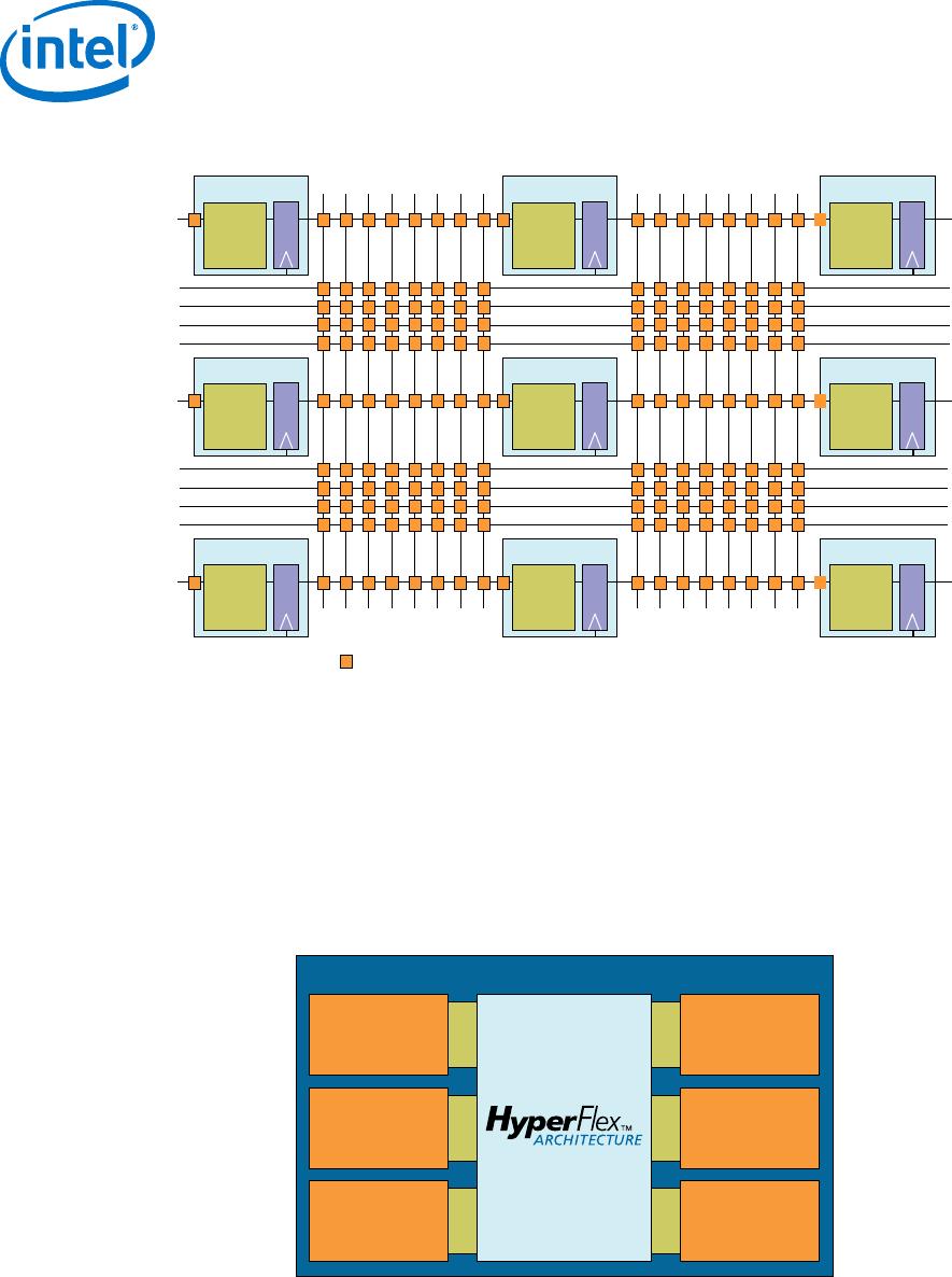
Within each transceiver tile, the transceivers are arranged in four banks of six PMA-
PCS groups. A wide variety of bonded and non-bonded data rate configurations are
possible within each bank, and within each tile, using a highly configurable clock
distribution network.
1.8.1. PMA Features
PMA channels are comprised of transmitter (TX), receiver (RX), and high speed
clocking resources.
Intel Stratix 10 device features provide exceptional signal integrity at data rates up to
28.3 Gbps. Clocking options include ultra-low jitter LC tank-based (ATX) PLLs with
optional fractional synthesis capability, channel PLLs operating as clock multiplier units
(CMUs), and fractional synthesis PLLs (fPLLs).
ATX PLL—can be configured in integer mode, or optionally, in a new fractional
synthesis mode. Each ATX PLL spans the full frequency range of the supported
data rate range providing a stable, flexible clock source with the lowest jitter.
CMU PLL—when not being used as a transceiver, select PMA channels can be
configured as channel PLLs operating as CMUs to provide an additional master
clock source within the transceiver bank.
fPLL—In addition, dedicated fPLLs are available with precision frequency synthesis
capabilities. fPLLs can be used to synthesize multiple clock frequencies from a
single reference clock source and replace multiple reference oscillators for multi-
protocol and multi-rate applications.
On the receiver side, each PMA has an independent channel PLL that allows analog
tracking for clock-data recovery. Each PMA also has advanced equalization circuits that
compensate for transmission losses across a wide frequency spectrum.
Variable Gain Amplifier (VGA)—to optimize the receiver's dynamic range
Continuous Time Linear Equalizer (CTLE)—to compensate for channel losses
with lowest power dissipation
Decision Feedback Equalizer (DFE)—to provide additional equalization
capability on backplanes even in the presence of crosstalk and reflections
On-Die Instrumentation (ODI)—to provide on-chip eye monitoring capabilities
(Eye Viewer). This capability helps to optimize link equalization parameters during
board bring-up and supports in-system link diagnostics and equalization margin
testing
1. Intel
®
Stratix
®
10 GX/SX Device Overview
S10-OVERVIEW | 2018.08.08
Stratix 10 GX/SX Device Overview
18

1SX250LH3F55I2LG

Mfr. #:
Manufacturer:
Intel / Altera
Description:
FPGA - Field Programmable Gate Array
Lifecycle:
New from this manufacturer.
Delivery:
DHL FedEx Ups TNT EMS
Payment:
T/T Paypal Visa MoneyGram Western Union