The core clock network in Intel Stratix 10 devices supports the new HyperFlex core
architecture at clock rates up to 1 GHz. It also supports the hard memory controllers
up to 2666 Mbps with a quarter rate transfer to the core. The core clock network is
supported by dedicated clock input pins, fractional clock synthesis PLLs, and integer
I/O PLLs.
1.15. Fractional Synthesis PLLs and I/O PLLs
Intel Stratix 10 devices have up to 32 fractional synthesis PLLs (fPLL) available for use
with transceivers or in the core fabric.
The fPLLs are located in the 3D SiP transceiver H-tiles, eight per tile, adjacent to the
transceiver channels. The fPLLs can be used to reduce both the number of oscillators
required on the board and the number of clock pins required, by synthesizing multiple
clock frequencies from a single reference clock source. In addition to synthesizing
reference clock frequencies for the transceiver transmit PLLs, the fPLLs can also be
used directly for transmit clocking. Each fPLL can be independently configured for
conventional integer mode, or enhanced fractional synthesis mode with third-order
delta-sigma modulation.
In addition to the fPLLs, Intel Stratix 10 devices contain up to 34 integer I/O PLLs
(IOPLLs) available for general purpose use in the core fabric and for simplifying the
design of external memory interfaces and high-speed LVDS interfaces. The IOPLLs are
located in each bank of 48 general purpose I/O, 1 per I/O bank, adjacent to the hard
memory controllers and LVDS SerDes in each I/O bank. This makes it easier to close
timing because the IOPLLs are tightly coupled with the I/Os that need to use them.
The IOPLLs can be used for general purpose applications in the core such as clock
network delay compensation and zero-delay clock buffering.
1.16. Internal Embedded Memory
Intel Stratix 10 devices contain two types of embedded memory blocks: M20K (20-
Kbit) and MLAB (640-bit).
The M20K and MLAB blocks are familiar block sizes carried over from previous Intel
device families. The MLAB blocks are ideal for wide and shallow memories, while the
M20K blocks are intended to support larger memory configurations and include hard
ECC. Both M20K and MLAB embedded memory blocks can be configured as a single-
port or dual-port RAM, FIFO, ROM, or shift register. These memory blocks are highly
flexible and support a number of memory configurations as shown in Table 11 on page
25.
Table 11. Internal Embedded Memory Block Configurations
MLAB (640 bits) M20K (20 Kbits)
64 x 10 (supported through emulation)
32 x 20
2K x 10 (or x8)
1K x 20 (or x16)
512 x 40 (or x32)
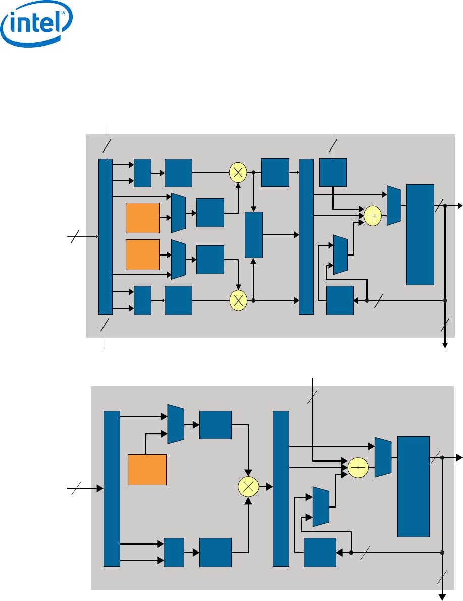
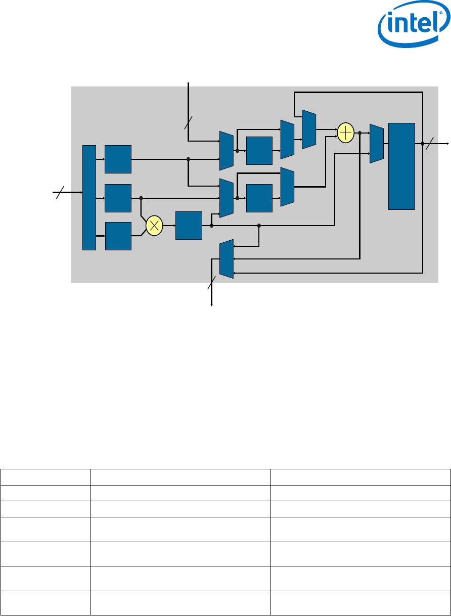
1.17. Variable Precision DSP Block
The Intel Stratix 10 DSP blocks are based upon the Variable Precision DSP
Architecture used in Intel’s previous generation devices. They feature hard fixed point
and IEEE-754 compliant floating point capability.
1. Intel
®
Stratix
®
10 GX/SX Device Overview
S10-OVERVIEW | 2018.08.08
Stratix 10 GX/SX Device Overview
25