Complex multiplication is very common in DSP algorithms. One of the most popular
applications of complex multipliers is the FFT algorithm. This algorithm has the
characteristic of increasing precision requirements on only one side of the multiplier.
The Variable Precision DSP block supports the FFT algorithm with proportional increase
in DSP resources as the precision grows.
Table 13. Complex Multiplication With Variable Precision DSP Block
Complex Multiplier
Size
DSP Block Resources FFT Usage
18x19 bits 2 Variable Precision DSP Blocks Resource optimized FFT
27x27 bits 4 Variable Precision DSP Blocks Highest precision FFT
For FFT applications with high dynamic range requirements, the Intel FFT IP Core
offers an option of single precision floating point implementation with resource usage
and performance similar to high precision fixed point implementations.
Other features of the DSP block include:
Hard 18-bit and 25-bit pre-adders
Hard floating point multipliers and adders
64-bit dual accumulator (for separate I, Q product accumulations)
Cascaded output adder chains for 18- and 27-bit FIR filters
Embedded coefficient registers for 18- and 27-bit coefficients
Fully independent multiplier outputs
Inferability using HDL templates supplied by the Intel Quartus Prime software for
most modes
The Variable Precision DSP block is ideal to support the growing trend towards higher
bit precision in high performance DSP applications. At the same time, it can efficiently
support the many existing 18-bit DSP applications, such as high definition video
processing and remote radio heads. With the Variable Precision DSP block architecture
and hard floating point multipliers and adders, Intel Stratix 10 devices can efficiently
support many different precision levels up to and including floating point
implementations. This flexibility can result in increased system performance, reduced
power consumption, and reduce architecture constraints on system algorithm
designers.
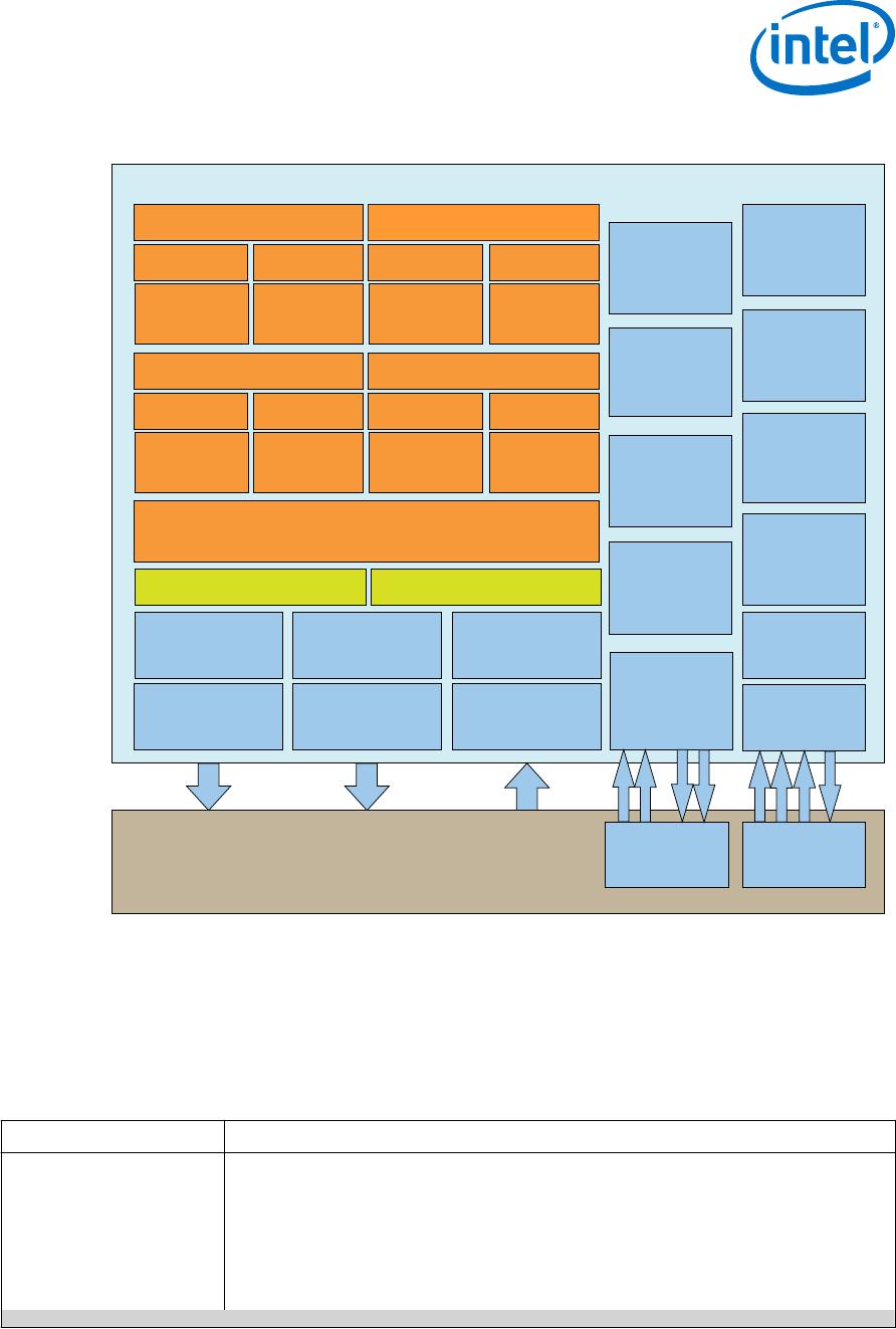
1.18. Hard Processor System (HPS)
The Intel Stratix 10 SoC Hard Processor System (HPS) is Intel’s industry leading third
generation HPS. Leveraging the performance of Intel’s 14-nm Tri-Gate technology,
Intel Stratix 10 SoC devices more than double the performance of previous generation
SoCs with an integrated quad-core 64-bit ARM Cortex-A53. The HPS also enables
system-wide hardware virtualization capabilities by adding a system memory
management unit. These architecture improvements ensure that Intel Stratix 10 SoCs
will meet the requirements of current and future embedded markets, including
wireless and wireline communications, data center acceleration, and numerous
military applications.
1. Intel
®
Stratix
®
10 GX/SX Device Overview
S10-OVERVIEW | 2018.08.08
Stratix 10 GX/SX Device Overview
28
Figure 13. HPS Block Diagram
Quad ARM Cortex-A53-Based Hard Processor System
1 MB L2 Cache with ECC
JTAG Debug
or Trace
256 KB
RAM
Timers
(x8)
HPS-to-FPGA
BRIDGE
FPGA-to-HPS
BRIDGE
SD/SDIO/
MMC
USB OTG
(x2)
DMA
(8 Channel)
UART (x2)
HPS IO
I
2
C (x5)
NAND
Flash
1, 2
EMAC (x3)
SPI (x4)
SDRAM
Scheduler
3
HPS-to-SDM
SDM-to-HPS
Notes:
1. Integrated direct memory access (DMA)
2. Integrated error correction code (ECC)
3. Multiport front-end interface to hard memory controller
System MMU Cache Coherency Unit
ARM Cortex -A53
NEON FPU
32 KB I-Cache
with Parity
32 KB D-Cache
with ECC
ARM Cortex -A53
NEON FPU
32 KB I-Cache
with Parity
32 KB D -Cache
with ECC
ARM Cortex -A53
NEON FPU
32 KB I-Cache
with Parity
32 KB D-Cache
with ECC
ARM Cortex -A53
NEON FPU
32 KB I-Cache
with Parity
32 KB D-Cache
with ECC
SDM
Hard Memory
Controller
FPGA Fabric
Lightweight HPS-to-
FPGA BRIDGE
2
1, 2
1, 2
2
1, 2
1.18.1. Key Features of the Intel Stratix 10 HPS
Table 14. Key Features of the Intel Stratix 10 GX/SX HPS
Feature Description
Quad-core ARM Cortex-A53
MPCore processor unit
2.3 MIPS/MHz instruction efficiency
CPU frequency up to 1.5 GHz
At 1.5 GHz total performance of 13,800 MIPS
ARMv8-A architecture
Runs 64-bit and 32-bit ARM instructions
16-bit and 32-bit Thumb instructions for 30% reduction in memory footprint
Jazelle
®
RCT execution architecture with 8-bit Java bytecodes
continued...
1. Intel
®
Stratix
®
10 GX/SX Device Overview
S10-OVERVIEW | 2018.08.08
Stratix 10 GX/SX Device Overview
29
Feature Description
Superscalar, variable length, out-of-order pipeline with dynamic branch prediction
Improved ARM NEON
media processing engine
Single- and double-precision floating-point unit
CoreSight
debug and trace technology
System Memory
Management Unit
Enables a unified memory model and extends hardware virtualization into peripherals
implemented in the FPGA fabric
Cache Coherency unit Changes in shared data stored in cache are propagated throughout the system
providing bi-directional coherency for co-processing elements.
Cache L1 Cache
32 KB of instruction cache w/ parity check
32 KB of L1 data cache w /ECC
Parity checking
L2 Cache
1MB shared
8-way set associative
SEU Protection with parity on TAG ram and ECC on data RAM
Cache lockdown support
On-Chip Memory 256 KB of scratch on-chip RAM
External SDRAM and Flash
Memory Interfaces for HPS
Hard memory controller with support for DDR4, DDR3, LPDDR3
40-bit (32-bit + 8-bit ECC) with select packages supporting 72-bit (64-bit + 8-bit
ECC)
Support for up to 2666 Mbps DDR4 and 2166 Mbps DDR3 frequencies
Error correction code (ECC) support including calculation, error correction, write-
back correction, and error counters
Software Configurable Priority Scheduling on individual SDRAM bursts
Fully programmable timing parameter support for all JEDEC-specified timing
parameters
Multiport front-end (MPFE) scheduler interface to the hard memory controller, which
supports the AXI
®
Quality of Service (QoS) for interface to the FPGA fabric
NAND flash controller
ONFI 1.0
Integrated descriptor based with DMA
Programmable hardware ECC support
Support for 8- and 16-bit Flash devices
Secure Digital SD/SDIO/MMC controller
eMMC 4.5
Integrated descriptor based DMA
CE-ATA digital commands supported
50 MHz operating frequency
Direct memory access (DMA) controller
8-channel
Supports up to 32 peripheral handshake interface
continued...
1. Intel
®
Stratix
®
10 GX/SX Device Overview
S10-OVERVIEW | 2018.08.08
Stratix 10 GX/SX Device Overview
30

1SX250LH3F55I2LG

Mfr. #:
Manufacturer:
Intel / Altera
Description:
FPGA - Field Programmable Gate Array
Lifecycle:
New from this manufacturer.
Delivery:
DHL FedEx Ups TNT EMS
Payment:
T/T Paypal Visa MoneyGram Western Union