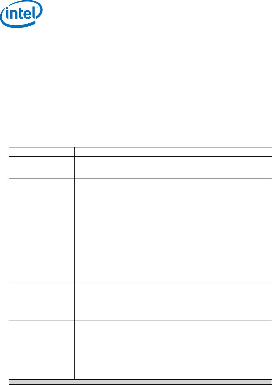
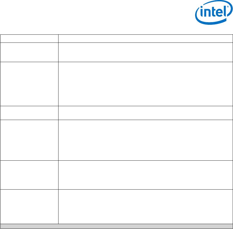
Feature Stratix V FPGAs Intel Stratix 10 FPGAs and SoCs
Logic density 952 KLE (monolithic) 5,500 KLE (monolithic)
Embedded memory (M20K) 52 Mbits 229 Mbits
18x19 multipliers 3,926
Note: Multiplier is 18x18 in
Stratix V devices.
11,520
Note: Multiplier is 18x19 in Intel
Stratix 10 devices.
Floating point DSP capability Up to 1 TFLOP, requires soft
floating point adder and
multiplier
Up to 10 TFLOPS, hard IEEE 754
compliant single precision floating
point adder and multiplier
Maximum transceivers 66 96
Maximum transceiver data rate (chip-to-
chip)
28.05 Gbps 28.3 Gbps L-Tile
28.3 Gbps H-Tile
Maximum transceiver data rate (backplane) 12.5 Gbps 12.5 Gbps L-Tile
28.3 Gbps H-Tile
Hard memory controller None DDR4 @ 1333 MHz/2666 Mbps
DDR3 @ 1067 MHz/2133 Mbps
Hard protocol IP PCIe Gen3 x8 (up to 4
instances)
PCIe Gen3 x16 (up to 4 instances)
SR-IOV (4 physical functions / 2k
virtual functions) on H-Tile devices
10GBASE-KR/40GBASE-KR4 FEC
Core clocking and PLLs Global, quadrant and regional
clocks supported by fractional-
synthesis fPLLs
Programmable clock tree synthesis
supported by fractional synthesis
fPLLs and integer IO PLLs
Register state readback and writeback Not available Non-destructive register state
readback and writeback for ASIC
prototyping and other applications
These innovations result in the following improvements:
Improved Core Logic Performance: The HyperFlex core architecture combined
with Intel’s 14-nm Tri-Gate technology allows Intel Stratix 10 devices to achieve
2X the core performance compared to the previous generation
Lower Power: Intel Stratix 10 devices use up to 70% lower power compared to
the previous generation, enabled by 14-nm Intel Tri-Gate technology, the
HyperFlex core architecture, and optional power saving features built into the
architecture
Higher Density: Intel Stratix 10 devices offer over five times the level of
integration, with up to 5,500K logic elements (LEs) in a monolithic fabric, over 229
Mbits of embedded memory blocks (M20K), and 11,520 18x19 multipliers
Embedded Processing: Intel Stratix 10 SoCs feature a Quad-Core 64-bit ARM
Cortex-A53 processor optimized for power efficiency and software compatible with
previous generation Arria and Cyclone SoC devices
Improved Transceiver Performance: With up to 96 transceiver channels
implemented in heterogeneous 3D SiP transceiver tiles, Intel Stratix 10 GX and SX
devices support data rates up to 28.3 Gbps chip-to-chip and 28.3 Gbps across the
backplane with signal conditioning circuits capable of equalizing over 30 dB of
system loss
Improved DSP Performance: The variable precision DSP block in Intel Stratix
10 devices features hard fixed and floating point capability, with up to 10
TeraFLOPS IEEE754 single-precision floating point performance
1. Intel
®
Stratix
®
10 GX/SX Device Overview
S10-OVERVIEW | 2018.08.08
Stratix 10 GX/SX Device Overview
7
Additional Hard IP: Intel Stratix 10 devices include many more hard IP blocks
than previous generation devices, with a hard memory controller included in each
bank of 48 general purpose IOs, a hard PCIe Gen3 x16 full protocol stack in each
transceiver tile, and a hard 10GBASE-KR/40GBASE-KR4 FEC in every transceiver
channel
Enhanced Core Clocking: Intel Stratix 10 devices feature programmable clock
tree synthesis; clock trees are only synthesized where needed, increasing the
flexibility and reducing the power dissipation of the clocking solution
Additional Core PLLs: The core fabric in Intel Stratix 10 devices is supported by
both integer IO PLLs and fractional synthesis fPLLs, resulting in a greater total
number of PLLs available than the previous generation
1.3. FPGA and SoC Features Summary
Table 2. Intel Stratix 10 FPGA and SoC Common Device Features
Feature Description
Technology 14-nm Intel Tri-Gate (FinFET) process technology
SmartVID controlled core voltage, standard power devices
0.85-V fixed core voltage, low static power devices available
Low power serial
transceivers
Up to 96 total transceivers available
Continuous operating range of 1 Gbps to 28.3 Gbps for Intel Stratix 10 GX/SX devices
Backplane support up to 28.3 Gbps for Intel Stratix 10 GX/SX devices
Extended range down to 125 Mbps with oversampling
ATX transmit PLLs with user-configurable fractional synthesis capability
XFP, SFP+, QSFP/QSFP28, CFP/CFP2/CFP4 optical module support
Adaptive linear and decision feedback equalization
Transmit pre-emphasis and de-emphasis
Dynamic partial reconfiguration of individual transceiver channels
On-chip instrumentation (Eye Viewer non-intrusive data eye monitoring)
General purpose I/Os Up to 1640 total GPIO available
1.6 Gbps LVDS—every pair can be configured as an input or output
1333 MHz/2666 Mbps DDR4 external memory interface
1067 MHz/2133 Mbps DDR3 external memory interface
1.2 V to 3.0 V single-ended LVCMOS/LVTTL interfacing
On-chip termination (OCT)
Embedded hard IP PCIe Gen1/Gen2/Gen3 complete protocol stack, x1/x2/x4/x8/x16 end point and root
port
DDR4/DDR3/LPDDR3 hard memory controller (RLDRAM3/QDR II+/QDR IV using soft
memory controller)
Multiple hard IP instantiations in each device
Single Root I/O Virtualization (SR-IOV)
Transceiver hard IP 10GBASE-KR/40GBASE-KR4 Forward Error Correction (FEC)
10G Ethernet PCS
PCI Express PIPE interface
Interlaken PCS
Gigabit Ethernet PCS
Deterministic latency support for Common Public Radio Interface (CPRI) PCS
Fast lock-time support for Gigabit Passive Optical Networking (GPON) PCS
8B/10B, 64B/66B, 64B/67B encoders and decoders
Custom mode support for proprietary protocols
continued...
1. Intel
®
Stratix
®
10 GX/SX Device Overview
S10-OVERVIEW | 2018.08.08
Stratix 10 GX/SX Device Overview
8
Feature Description
Power management SmartVID controlled core voltage, standard power devices
0.85-V fixed core voltage, low static power devices available
Intel Quartus
®
Prime Pro Edition integrated power analysis
High performance monolithic
core fabric
HyperFlex core architecture with Hyper-Registers throughout the interconnect routing
and at the inputs of all functional blocks
Monolithic fabric minimizes compile times and increases logic utilization
Enhanced adaptive logic module (ALM)
Improved multi-track routing architecture reduces congestion and improves compile
times
Hierarchical core clocking architecture with programmable clock tree synthesis
Fine-grained partial reconfiguration
Internal memory blocks M20K—20-Kbit with hard ECC support
MLAB—640-bit distributed LUTRAM
Variable precision DSP
blocks
IEEE 754-compliant hard single-precision floating point capability
Supports signal processing with precision ranging from 18x19 up to 54x54
Native 27x27 and 18x19 multiply modes
64-bit accumulator and cascade for systolic FIRs
Internal coefficient memory banks
Pre-adder/subtractor improves efficiency
Additional pipeline register increases performance and reduces power
Phase locked loops (PLL) Fractional synthesis PLLs (fPLL) support both fractional and integer modes
Fractional mode with third-order delta-sigma modulation
Precision frequency synthesis
Integer PLLs adjacent to general purpose I/Os, support external memory, and LVDS
interfaces, clock delay compensation, zero delay buffering
Core clock networks 1 GHz fabric clocking
667 MHz external memory interface clocking, supports 2666 Mbps DDR4 interface
800 MHz LVDS interface clocking, supports 1600 Mbps LVDS interface
Programmable clock tree synthesis, backwards compatible with global, regional and
peripheral clock networks
Clocks only synthesized where needed, to minimize dynamic power
continued...
1. Intel
®
Stratix
®
10 GX/SX Device Overview
S10-OVERVIEW | 2018.08.08
Stratix 10 GX/SX Device Overview
9

1SX250LH3F55I2LG

Mfr. #:
Manufacturer:
Intel / Altera
Description:
FPGA - Field Programmable Gate Array
Lifecycle:
New from this manufacturer.
Delivery:
DHL FedEx Ups TNT EMS
Payment:
T/T Paypal Visa MoneyGram Western Union