P6SMB540A

Features
n RoHS compliant* and halogen free**
n Surface Mount SMB package
n Breakdown Voltage: 6.8 to 550 volts
n Peak Pulse Power: 600 watts
n Typical temperature coefficient:
V
BR
= 0.1 % x V
BR
@ 25 °C x T
Applications
n IEC 61000-4-2 ESD (Min. Level 4)
n IEC 61000-4-4 EFT
n IEC 61000-4-5 Surge
Maximum Characteristics (@ T
A
= 25 °C Unless Otherwise Noted)
P6SMB Transient Voltage Suppressor Diode Series
* RoHS Directive 2002/95/EC Jan. 27, 2003 including annex and RoHS Recast 2011/65/EU June 8, 2011.
**Bourns considers a product to be “halogen free” if (a) the Bromine (Br) content is 900 ppm or less; (b) the Chlorine (Cl) content is 900 ppm or less; and (c) the total Bromine (Br)
and Chlorine (Cl) content is 1500 ppm or less.
Specifications are subject to change without notice.
The device characteristics and parameters in this data sheet can and do vary in different applications and actual device performance may vary over time.
Users should verify actual device performance in their specific applications.
Parameter Symbol Value Unit
Peak Pulse Power Dissipation (T
P
= 1 ms)
(Note 1,2)
P
PK
600 Watts
Peak Forward Surge Current
8.3 ms Single Half Sine Wave Superimposed on Rated Load
(JEDEC Method)
(Note 3)
I
FSM
100 Amps
Maximum Instantaneous Forward Voltage @ I
PP
= 50 A
(For Unidirectional Units Only)
P6SMB6.8A ~ P6SMB200A
P6SMB220A ~ P6SMB550A
V
F
3.5
5.0
Volts
Operating Temperature Range T
J
-55 to +150 °C
Storage Temperature Range T
STG
-55 to +150 °C
1. Non-repetitive current pulse, per Pulse Waveform graph and derated above T
A
= 25 °C per Pulse Derating Curve.
2. Thermal Resistance Junction to Lead.
3. 8.3 ms Single Half-Sine Wave duty cycle = 4 pulses maximum per minute (unidirectional units only).
General Information
The markets of portable communications, computing and video equipment are challenging the semiconductor industry to develop
increasingly smaller electronic components.
Bourns offers Transient Voltage Suppressor Diodes for surge and ESD protection applications, in compact chip package DO-214AA (SMB)
size format. The Transient Voltage Suppressor series offers a choice of Breakdown Voltages from 6.8 V up to 550 V. Typical fast response
times are less than 1.0 picosecond for unidirectional devices and less than 5.0 picoseconds for bidirectional devices from 0 V to Minimum
Breakdown Voltage.
Bourns
®
Chip Diodes conform to JEDEC standards, are easy to handle with standard pick and place equipment and the at conguration
minimizes roll away.
How to Order
P6SMB 6.8 CA - H
Series
P6SMB= SMB/DO-214AA
Breakdown Voltage
6.8 to 550 = 6.8 to 550 V
BD
(Volts)
Sufx
A = 5 % Tolerance Unidirectional Device
CA = 5 % Tolerance Bidirectional Device
Reel
(blank) = 13 inch reel
-H = 7 inch reel
*RoHS COMPLIANT
LEAD FREE
*RoHS COMPLIANT
VERSIONS
AVAILABLE
LEAD FREE
VERSIONS ARE
RoHS COMPLIANT*
Asia-Pacic:
Tel: +886-2 2562-4117
Email: asiacus@bourns.com
Europe:
Tel: +36 88 520 390
Email: eurocus@bourns.com
The Americas:
Tel: +1-951 781-5500
Email: americus@bourns.com
www.bourns.com
Specifications are subject to change without notice.
The device characteristics and parameters in this data sheet can and do vary in different applications and actual device performance may vary over time.
Users should verify actual device performance in their specific applications.
P6SMB Transient Voltage Suppressor Diode Series
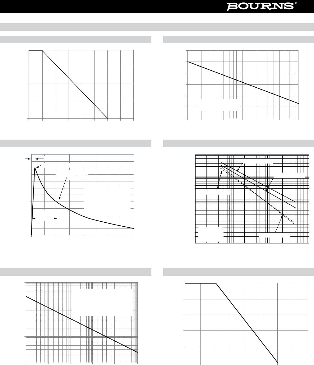
Electrical Characteristics (@ T
A
= 25 °C Unless Otherwise Noted)
Notes:
1. Sufx ‘A denotes a 5 % tolerance unidirectional device.
2. Sufx ‘CA denotes a 5 % tolerance bidirectional device.
3. For bidirectional devices with a V
R
of 10 volts or less, the I
R
limit is double.
Unidirectional Device Bidirectional Device
Breakdown Voltage
V
BR
(Volts)
Working
Peak
Reverse
Voltage
Maximum
Reverse
Leakage
@ V
RWM
Maximum
Reverse
Voltage
@ I
RSM
Maximum
Reverse
Surge
Current
Part No. Marking Part No. Marking Min. Max. @ I
T
(mA) V
RWM
(V) I
R
(μA) V
RSM
(V) I
RSM
(A)
P6SMB6.8A 6V8A P6SMB6.8CA 6V8C 6.45 7.14 10 5.8 1000 10.5 58.1
P6SMB7.5A 7V5A P6SMB7.5CA 7V5C 7.13 7.88 10 6.4 500 11.3 54
P6SMB8.2A 8V2A P6SMB8.2CA 8V2C 7.79 8.61 10 7.02 200 12.1 50.4
P6SMB9.1A 9V1A P6SMB9.1CA 9V1C 8.65 9.55 1 7.78 50 13.4 45.5
P6SMB10A 10A P6SMB10CA 10C 9.5 10.5 1 8.55 10 14.5 42.1
P6SMB11A 11A P6SMB11CA 11C 10.5 11.6 1 9.4 5 15.6 39.1
P6SMB12A 12A P6SMB12CA 12C 11.4 12.6 1 10.2 5 16.7 36.5
P6SMB13A 13A P6SMB13CA 13C 12.4 13.7 1 11.1 1 18.2 33.5
P6SMB15A 15A P6SMB15CA 15C 14.3 15.8 1 12.8 1 21.2 28.8
P6SMB16A 16A P6SMB16CA 16C 15.2 16.8 1 13.6 1 22.5 27.1
P6SMB18A 18A P6SMB18CA 18C 17.1 18.9 1 15.3 1 25.5 24.2
P6SMB20A 20A P6SMB20CA 20C 19 21 1 17.1 1 27.7 22
P6SMB22A 22A P6SMB22CA 22C 20.9 23.1 1 18.8 1 30.6 19.9
P6SMB24A 24A P6SMB24CA 24C 22.8 25.2 1 20.5 1 33.2 18.4
P6SMB27A 27A P6SMB27CA 27C 25.7 28.4 1 23.1 1 37.5 16.3
P6SMB30A 30A P6SMB30CA 30C 28.5 31.5 1 25.6 1 41.4 14.7
P6SMB33A 33A P6SMB33CA 33C 31.4 34.7 1 28.2 1 45.7 13.3
P6SMB36A 36A P6SMB36CA 36C 34.2 37.8 1 30.8 1 49.9 12.2
P6SMB39A 39A P6SMB39CA 39C 37.1 41 1 33.3 1 53.9 11.3
P6SMB43A 43A P6SMB43CA 43C 40.9 45.2 1 36.8 1 59.3 10.3
P6SMB47A 47A P6SMB47CA 47C 44.7 49.4 1 40.2 1 64.8 9.4
P6SMB51A 51A P6SMB51CA 51C 48.5 53.6 1 43.6 1 70.1 8.7
P6SMB56A 56A P6SMB56CA 56C 53.2 58.8 1 47.8 1 77 7.9
P6SMB62A 62A P6SMB62CA 62C 58.9 65.1 1 53 1 85 7.2
P6SMB68A 68A P6SMB68CA 68C 64.6 71.4 1 58.1 1 92 6.6
P6SMB75A 75A P6SMB75CA 75C 71.3 78.8 1 64.1 1 103 5.9
P6SMB82A 82A P6SMB82CA 82C 77.9 86.1 1 70.1 1 113 5.4
P6SMB91A 91A P6SMB91CA 91C 86.5 95.5 1 77.8 1 125 4.9
P6SMB100A 100A P6SMB100CA 100C 95 105 1 85.5 1 137 4.5
P6SMB110A 110A P6SMB110CA 110C 105 116 1 94 1 152 4
P6SMB120A 120A P6SMB120CA 120C 114 126 1 102 1 165 3.7
P6SMB130A 130A P6SMB130CA 130C 124 137 1
111 1 179 3.4
P6SMB150A 150A P6SMB150CA 150C 143 158 1 128 1 207 2.9
P6SMB160A 160A P6SMB160CA 160C 152 168 1 136 1 219 2.8
P6SMB170A 170A P6SMB170CA 170C 162 179 1 145 1 234 2.6
P6SMB180A 180A P6SMB180CA 180C 171 189 1 154 1 246 2.5
P6SMB200A 200A P6SMB200CA 200C 190 210 1 171 1 274 2.2
P6SMB220A 220A P6SMB220CA 220C 209 231 1 185 1 328 1.9
P6SMB250A 250A P6SMB250CA 250C 237 263 1 214 1 344 1.8
P6SMB300A 300A P6SMB300CA 300C 285 315 1 256 1 414 1.5
P6SMB350A 350A P6SMB350CA 350C 332 368 1 300 1 482 1.3
P6SMB400A 400A P6SMB400CA 400C 380 420 1 342 1 548 1.1
P6SMB440A 440A P6SMB440CA 440C 418 462 1 376 1 602 1
P6SMB480A 480A P6SMB480CA 480C 456 504 1 408 1 658 0.9
P6SMB510A 510A P6SMB510CA 510C 485 535 1 434 1 698 0.9
P6SMB530A 530A P6SMB530CA 530C 503.5 556.5 1 477 1 725 0.8
P6SMB540A 540A P6SMB540CA 540C 513 567 1 486 1 740 0.8
P6SMB550A 550A P6SMB550CA 550C 522.5 577.5 1 495 1 760 0.8
3312 - 2 mm SMD Trimming Potentiometer P6SMB Transient Voltage Suppressor Diode Series
Rating & Characteristic Curves
Pulse Derating Curve Maximum Non-Repetitive Surge Current
Pulse Waveform Typical Junction Capacitance
Pulse Rating Curve Steady State Power Derating Curve
100
75
50
25
0
050
25 75 100 150125 175 200
Ambient Temperature (
Peak Pulse Derating in Percent of
Peak Power or Current
°C)
5.0
3.0
4.0
2.0
1.0
0.0
05025 75 100 150125 175 200
TL, Lead Temperature (°C)
RM(AV) Steady State Power Dissipation (W)
60 Hz Resistive or
Inductive Load
100
50
0
0 1.0 2.0 3.0 4.0
T, Time (ms)
I
P
, Peak Pulse Current (%)
TA=25 °C
TP
TR=10 µs
Half value=
IRSM
2
Peak value (IRSM)
Pulse width (TP)
is defined as that point
where the peak current
decays to 50 % of IPSM.
10 x 1000 waveform
as defined by R.E.A.
Peak Forward Surge Current (Amps)
120
80
100
60
40
20
0
1 2510 20 50 100
Number of Cycles at 60 Hz
Pulse Width 8.3 ms
Single Half Sine-Wave
100
10
1.0
0.1
0.1 µs 1.0 µs 10 µs 10 ms
TP, Pulse Width
P
P
, Peak Power (KW)
100 µs 1.0 ms
TA = 25 °C
Non-repetitive
Pulse Waveform
Shown in Pulse Waveform Graph
1
10
100
1000
10000
101 100 1000
C
J
-
Junction Capacitance (pF)
Bidirectional V = 0 V
Unidirectional V = 0 V
Bidirectional @VR
Unidirectional @VR
T = 25 ° C
f = 1.0 MHz
Vsig = 50 mVp-p
V
BR
- Reverse Breakdown Voltage (V)
100
75
50
25
0
05025 75 100 150125 175 200
Ambient Temperature (
Peak Pulse Derating in Percent of
Peak Power or Current
°C)
5.0
3.0
4.0
2.0
1.0
0.0
05025 75 100 150125 175 200
TL, Lead Temperature (°C)
RM(AV) Steady State Power Dissipation (W)
60 Hz Resistive or
Inductive Load
100
50
0
0 1.0 2.0 3.0 4.0
T, Time (ms)
I
P
, Peak Pulse Current (%)
TA=25 °C
TP
TR=10 µs
Half value=
IRSM
2
Peak value (IRSM)
Pulse width (TP)
is defined as that point
where the peak current
decays to 50 % of IPSM.
10 x 1000 waveform
as defined by R.E.A.
Peak Forward Surge Current (Amps)
120
80
100
60
40
20
0
1
2510 20 50 100
Number of Cycles at 60 Hz
Pulse Width 8.3 ms
Single Half Sine-Wave
100
10
1.0
0.1
0.1 µs 1.0 µs 10 µs 10 ms
TP, Pulse Width
P
P
, Peak Power (KW)
100 µs 1.0 ms
TA = 25 °C
Non-repetitive
Pulse Waveform
Shown in Pulse Waveform Graph
1
10
100
1000
10000
101 100 1000
C
J
-
Junction Capacitance (pF)
Bidirectional V = 0 V
Unidirectional V = 0 V
Bidirectional @VR
Unidirectional @VR
T = 25 ° C
f = 1.0 MHz
Vsig = 50 mVp-p
V
BR
- Reverse Breakdown Voltage (V)
100
75
50
25
0
05025 75 100 150125 175 200
Ambient Temperature (
Peak Pulse Derating in Percent of
Peak Power or Current
°C)
5.0
3.0
4.0
2.0
1.0
0.0
05025 75 100 150125 175 200
TL, Lead Temperature (°C)
RM(AV) Steady State Power Dissipation (W)
60 Hz Resistive or
Inductive Load
100
50
0
0 1.0
2.0 3.0 4.0
T, Time (ms)
I
P
, Peak Pulse Current (%)
TA=25 °C
TP
TR=10 µs
Half value=
IRSM
2
Peak value (IRSM)
Pulse width (TP)
is defined as that point
where the peak current
decays to 50 % of IPSM.
10 x 1000 waveform
as defined by R.E.A.
Peak Forward Surge Current (Amps)
120
80
100
60
40
20
0
1 2510 20 50 100
Number of Cycles at 60 Hz
Pulse Width 8.3 ms
Single Half Sine-Wave
100
10
1.0
0.1
0.1 µs 1.0 µs 10 µs 10 ms
TP, Pulse Width
P
P
, Peak Power (KW)
100 µs 1.0 ms
TA = 25 °C
Non-repetitive
Pulse Waveform
Shown in Pulse Waveform Graph
1
10
100
1000
10000
101 100 1000
C
J
-
Junction Capacitance (pF)
Bidirectional V = 0 V
Unidirectional V = 0 V
Bidirectional @VR
Unidirectional @VR
T = 25 ° C
f = 1.0 MHz
Vsig = 50 mVp-p
V
BR
- Reverse Breakdown Voltage (V)
100
75
50
25
0
05025 75 100 150125 175 200
Ambient Temperature (
Peak Pulse Derating in Percent of
Peak Power or Current
°C)
5.0
3.0
4.0
2.0
1.0
0.0
05025 75 100 150125 175 200
TL, Lead Temperature (°C)
RM(AV) Steady State Power Dissipation (W)
60 Hz Resistive or
Inductive Load
100
50
0
0 1.0 2.0 3.0 4.0
T, Time (ms)
I
P
, Peak Pulse Current (%)
TA=25 °C
TP
TR=10 µs
Half value=
IRSM
2
Peak value (IRSM)
Pulse width (TP)
is defined as that point
where the peak current
decays to 50 % of IPSM.
10 x 1000 waveform
as defined by R.E.A.
Peak Forward Surge Current (Amps)
120
80
100
60
40
20
0
1 2510 20 50 100
Number of Cycles at 60 Hz
Pulse Width 8.3 ms
Single Half Sine-Wave
100
10
1.0
0.1
0.1 µs
1.0 µs 10 µs 10 ms
TP, Pulse Width
P
P
, Peak Power (KW)
100 µs 1.0 ms
TA = 25 °C
Non-repetitive
Pulse Waveform
Shown in Pulse Waveform Graph
1
10
100
1000
10000
101 100 1000
C
J
-
Junction Capacitance (pF)
Bidirectional V = 0 V
Unidirectional V = 0 V
Bidirectional @VR
Unidirectional @VR
T = 25 ° C
f = 1.0 MHz
Vsig = 50 mVp-p
V
BR
- Reverse Breakdown Voltage (V)
5.0
3.0
4.0
2.0
1.0
0.0
050
25 75 100 150125 175 200
TL, Lead Temperature (°C)
RM(AV) Steady State Power Dissipation (W)
60 Hz Resistive or
Inductive Load
Specifications are subject to change without notice.
The device characteristics and parameters in this data sheet can and do vary in different applications and actual device performance may vary over time.
Users should verify actual device performance in their specific applications.

P6SMB540A

Mfr. #:
Manufacturer:
Littelfuse
Description:
TVS Diodes / ESD Suppressors 600W 540V 5% Uni-Directional
Lifecycle:
New from this manufacturer.
Delivery:
DHL FedEx Ups TNT EMS
Payment:
T/T Paypal Visa MoneyGram Western Union