1
Power Factor Correction Controllers
ISL6730A, ISL6730B, ISL6730C, ISL6730D
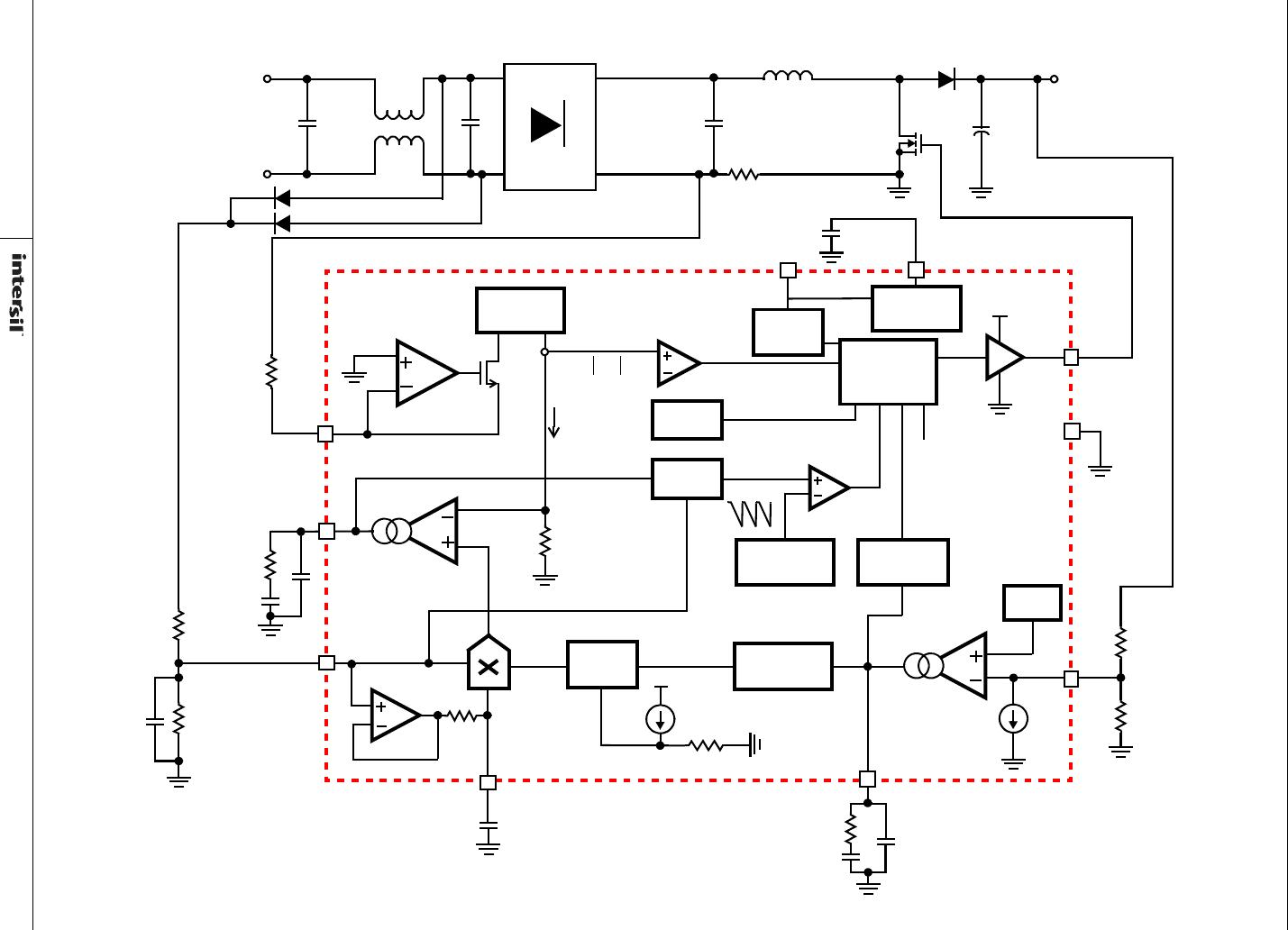
The ISL6730A, ISL6730B, ISL6730C, ISL6730D are active
Power Factor Correction (PFC) controller ICs that use a boost
topology. The controllers are suitable for AC/DC power
systems, up to 2kW and over the universal line input.
The ISL6730A, ISL6730B, ISL6730C, ISL6730D operate in
Continuous Conduction Mode (CCM). Accurate input current
shaping is achieved with a current error amplifier. A patent
pending breakthrough negative capacitance technology
minimizes zero crossing distortion and reduces the magnetic
components size. The small external components result in a
low cost design without sacrificing performance.
The internally clamped 12.5V gate driver delivers 1.5A peak
current to the external power MOSFET. The ISL6730A,
ISL6730B, ISL6730C, ISL6730D provide a highly reliable
system that is fully protected. Protection features include
cycle-by-cycle overcurrent, over power limit, over-temperature,
input brownout, output overvoltage and undervoltage
protection.
The ISL6730A, ISL6730B provide excellent power efficiency
and transitions into a power saving skip mode during light load
conditions, thus improving efficiency automatically. The
ISL6730A, ISL6730B, ISL6730C, ISL6730D can be shut down
by pulling the FB pin below 0.5V or grounding the BO pin. The
ISL6730C, ISL6730D have no skip mode.
Two switching frequency options are provided. The ISL6730B,
ISL6730D switch at 62kHz, and the ISL6730A, ISL6730C
switch at 124kHz.
Features
Reduce component size requirements
- Enables smaller, thinner AC/DC adapters
- Choke and cap size can be reduced
- Lower cost of materials
Excellent power factor over line and load regulation
- Internal current compensation
- CCM Mode with Patent pending IP for smaller EMI filter
•Better light load efficiency
- Automatic pulse skipping
- Programmable or automatic shutdown
High reliable design
- Cycle-by-cycle current limit
- Input average power limit
- OVP and OTP protection
- Input brownout protection
Small 10 Ld MSOP package
Applications
Desktop computer AC/DC adaptor
Laptop computer AC/DC adaptor
•TV AC/DC power supply
•AC/DC brick converters
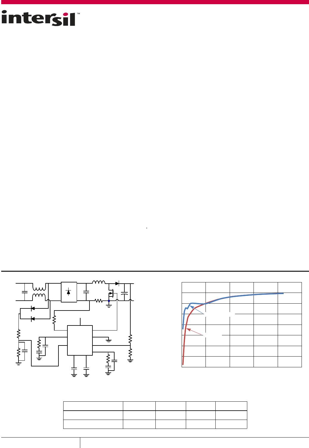
FIGURE 1. TYPICAL APPLICATION FIGURE 2. PFC EFFICIENCY
+
ISL6730
VCC
ISEN
ICOMP
VIN
GATE
GND
FB
BO VREG
COMP
V
LINE
V
OUT
V
I
OUTPUT POWER (W)
EFFICIENCY (%)
ISL6730C
ISL6730A, SKIP
100
95
60
65
70
90
85
80
75
0 20 40 60 80 100
TABLE 1. KEY DIFFERENCES IN FAMILY OF ISL6730
VERSION ISL6730A ISL6730B ISL6730C ISL6730D
Switching Frequency 124kHz 62kHz 124kHz 62kHz
Skip Mode Yes-Fixed Yes-Fixed No No
August 8, 2013
FN8258.1
CAUTION: These devices are sensitive to electrostatic discharge; follow proper IC Handling Procedures.
1-888-INTERSIL or 1-888-468-3774
| Copyright Intersil Americas LLC 2013. All Rights Reserved
Intersil (and design) is a trademark owned by Intersil Corporation or one of its subsidiaries.
All other trademarks mentioned are the property of their respective owners.
ISL6730A, ISL6730B, ISL6730C, ISL6730D
2
FN8258.1
August 8, 2013
Pin Configuration
ISL6730A, ISL6730B, ISL6730C, ISL6730D
(10 LD MSOP)
TOP VIEW
7
8
10
9
4
3
2
1
GND
ISEN
ICOMP
VIN
GATE
VREG
FB
VCC
65
BO
COMP
Pin Descriptions
PIN # I/O SYMBOL DESCRIPTION
1 - GND Ground pin. All voltage levels refer to this pin.
2 I ISEN Current sense pin. The current through this pin is proportional to the inductor current.
3 I/O ICOMP Current error amplifier output pin.
4 I VIN Input voltage sense. This pin provides the reference voltage to shape inductor current. Connect this pin to a resistor divider from
the rectified input voltage. The resistor divider ratio is used to adjust the phase lag between input voltage and the input current.
The phase lag is required to compensate the phase lead generated by the EMI filter.
5 I/O BO This pin should be decoupled to GND with a minimum 0.1µF ceramic capacitor. The BO pin is a voltage follower, which will follow
the DC voltage of the VIN pin. The BO pin is internally tied to GND through a resistor R
IS
. The decoupling capacitor provides ripple
filtering. When the voltage at the BO pin (V
BO
) drops below brownout voltage threshold, the controller enters shutdown mode
and the gate drive is disabled. The BO pin will be disabled when the FB pin drops below the enabling threshold.
6 I/O COMP Output of the error amplifier. The voltage of the COMP pin sets the input power. During start-up, a small charge current will slowly
ramp up the voltage of the COMP pin.
7 I FB Voltage feed back pin. Connect this pin to a resistor divider from the output. The resistor divider sets the output voltage. When
the FB pin voltage exceeds 104% of the reference voltage, overvoltage-protection is triggered and gate drive is disabled. When
the FB pin is below 10%, the device is put into shutdown mode. There is an internal pull-down current source for open loop
protection.
8 - VREG Output of internal regulator. The voltage having a ±2% tolerance over line, load and operating temperature. Bypass to GND with
a 47nF low ESR capacitor. VREG can source up to 10mA. This pin is not recommended for usage other than bypass.
9 I VCC Power supply pin. The VCC pin should be decoupled to GND with a minimum 0.1µF ceramic capacitor.
10 O GATE Push-pull gate drive for the external MOSFET. Output voltage is clamped at 12.5V. This pin provides typically 2A sink and 1.5A
source capability.
Ordering Information
PART NUMBER
(Notes 1, 2, 3)
PART
MARKING
TEMP.
RANGE (°C)
PACKAGE
(Pb-Free)
PKG.
DWG. #
ISL6730AFUZ 6730A -40 to +125 10 Ld MSOP M10.118
ISL6730BFUZ 6730B -40 to +125 10 Ld MSOP M10.118
ISL6730CFUZ 6730C -40 to +125 10 Ld MSOP M10.118
ISL6730DFUZ 6730D -40 to +125 10 Ld MSOP M10.118
ISL6730AEVAL1Z Evaluation Board
ISL6730BEVAL1Z Evaluation Board
NOTES:
1. Add “-T*” suffix for tape and reel. Please refer to TB347
for details on reel specifications.
2. These Intersil Pb-free plastic packaged products employ special Pb-free material sets, molding compounds/die attach materials, and 100% matte
tin plate plus anneal (e3 termination finish, which is RoHS compliant and compatible with both SnPb and Pb-free soldering operations). Intersil
Pb-free products are MSL classified at Pb-free peak reflow temperatures that meet or exceed the Pb-free requirements of IPC/JEDEC J STD-020.
3. For Moisture Sensitivity Level (MSL), please see device information page. For more information on MSL please see techbrief TB363
.
ISL6730A, ISL6730B, ISL6730C, ISL6730D
3
FN8258.1
August 8, 2013
Block Diagram
FB
COMP
GATE
PWM
VCC
CONTROL
LOGIC
VIN
ISEN
OSCILLATOR
COMP
GND
OTP
VCC
BO
I
FB
R
SEN
R
IS
ICOMP
I
REF
CEQ GEN.
CURRENT
MIRROR
OVER POWER
LIMIT
SOFT-START
ENABLE
2.5V
SKIP
20µA
SKIP
CLAMP
SKIP
2:1
0.25 VIN
×
BO
2
----------------------------- C O M P B
Q
1
C
OUT
V
OUT
L
COMP-1V
R
CS
V
CS
R
IS
I
ISEN
×
2
-----------------------------------=
C
F1
V
LINE
C
F3
EMI CHOKE
UVLO
R
FB1
R
FB2
L
m
R
IN2
C
BO
R
IN1
D
I
CS
I
OC
2
-------------->
I
CS
COMPB
D
F1
D
F2
C
REG
LINEAR
REGULATOR
VREG
V
I
Gmi
Gmv
C
F2

ISL6730DFUZ

Mfr. #:
Manufacturer:
Renesas / Intersil
Description:
Power Factor Correction - PFC PFC Controller
Lifecycle:
New from this manufacturer.
Delivery:
DHL FedEx Ups TNT EMS
Payment:
T/T Paypal Visa MoneyGram Western Union