ISL6730A, ISL6730B, ISL6730C, ISL6730D
10
FN8258.1
August 8, 2013
Functional Description
VCC Undervoltage Lockout (UVLO)
The ISL6730A, ISL6730B, ISL6730C, ISL6730D start
automatically once the voltage at VCC exceeds the UVLO
threshold.
Shutdown
When the VFB pin is below 0.2V, the controller is disabled and
the PWM output driver is tri-stated. When disabled, the IC power
will be reduced. During shutdown, the COMP pin is discharged to
GND and the controller is disabled. The Over-Temperature
Protection (OTP) is still alive to prevent the controller from
starting up in a high temperature ambient condition.
In the event that the FB pin is disconnected from the feedback
resistors, the FB pin is pulled to ground by an internal current
source I
FB
. When the FB pin voltage drops below 0.2V, the gate
driver is disabled. The ISL6730A, ISL6730B, ISL6730C,
ISL6730D enters shutdown mode.
Soft-Start
The COMP pin is released once the soft-start operation begins. A
13µA current sources out to the RC network connected from the
COMP pin until the FB pin voltage reaches 90% of the reference
voltage.
Switching is inhibited when the COMP pin voltage is below 1V.
When the COMP pin reaches 1V, the current error amplifier and
the gate driver are activated and the converter starts switching.
During UVLO, Brownout and Shutdown, the COMP is pulled to the
ground.
Input Voltage Sensing
The VIN pin is needed to sense the rectified input voltage. The
sensed semi-sinusoidal waveform is needed to shape inductor
current, which helps achieves unity power factor. At the same
time, the voltage on the VIN pin is used to generate the negative
capacitive element at the input. This will cancel the input filter
capacitor, C
F
. Canceling the effect of C
F
will increase the
displacement power factor and alleviate the zero crossing
distortion, which is related to the distortion power factor.
The BO pin also utilizes the VIN resistor divider for voltage
sensing. Set the resistor divider ratio to satisfy the brownout
requirement.
First, calculate the resistor divider ratio, K
BO
.
Where V
F
is the forward voltage drop of the bridge rectifier and
the voltage drop of D
F1;
D
F2
.
Then, select the R
IN2
based on the highest reasonable resistance
value. Then select the R
IN1
based upon the desirable minimum
RMS value of the line voltage for the PFC operation.
Inductor Current Sensing
The current sensing of the converter has two purposes. One is to
force the inductor current to track the input semi-sinusoidal
waveform. The other purpose is for overcurrent protection. Refer to
Figure 11 for the current sensing scheme. The sensed current I
CS
is in proportion to the inductor current, I
L
as described in
Equation 3.
where:
R
CS
is the current sensing resistor with low value in the return
path to the bridge rectifier.
R
SEN
is the current scaling resistor connected between ISEN to
the R
CS
.
FIGURE 10. INPUT VOLTAGE SENSING SCHEMATIC
BO
R
IN1
C
BO
VIN
C
F2
V
LINE
C
F3
EMI CHOKE
L
m
D
F1
D
F2
R
IN2
K
BO
V
BORMAX
V
RMSmin
2V
F
-------------------------------------------
=
(EQ. 1)
R
IN1
K
BO
1K
BO
---------------------
R
IN2
=
(EQ. 2)
I
CS
1
2
---
R
CS
R
SEN
----------------
I
L
⋅⋅=
(EQ. 3)
ISL6730A, ISL6730B, ISL6730C, ISL6730D
11
FN8258.1
August 8, 2013
A high value R
CS
renders more accurate current sensing. It is
recommended to use the R
CS
to render 120mV peak voltage at
the maximum line voltage during full load condition.
Where η is the efficiency of the converter at the maximum line
input with full load.
Since the R
CS
sees the average input current, high value R
CS
generates high power dissipation on the R
CS
. Use a reasonable
R
CS
according to the resistor power rating. The worst-case power
dissipation occurs at the input low line when input current is at
its maximum. Power dissipation by the resistor is:
where:
I
RMSMAX
is the maximum input RMS current at the minimum
input line voltage, V
RMSmin
.
Select the R
SEN
according to the peak current limit requirement.
The resistor is sized for an overload current 25% more than the
peak inductor peak current.
Negative Input Capacitor Generation (Patent
Pending)
The patent pending negative capacitor generation capability of
the ISL6730A, ISL6730B, ISL6730C, ISL6730D allows the
capacitor C
F2
to be moved from before the bridge rectifier
(Figure 12) to after the bridge rectifier (Figure 13). Thus, a
smaller lower cost C
F2
can be used. The change in topology
reduces the size of the EMI filter. Furthermore, C
F1
can be
increased thus decreasing the size of L
F
(Figure 13).
For applications where the output power is above 500W, the
negative capacitance helps to improve the power factor
dramatically. Please refer to Table 2 for the recommended
filtering capacitor to be placed after the bridge rectifier, C
F1
.
Additional C
F1
may be used to accommodate the use of small
boost inductor or to eliminate the differential mode filter inductor
as long as the equipment meets the power factor or goal.
The equivalent negative capacitor is a function of the input
voltage divider ratio, K
BO
, the current sensing gain and current
compensation error integration gain.
Adjusting the negative Ceq can be achieved by adjusting the
current compensation network.
Frequency Modulation
The ISL6730A, ISL6730B, ISL6730C, ISL6730D can further
reduce EMI filter size by lowering the differential noise power
density. The reduction is achieved by switching frequency
modulation.
The frequency varies with the VIN pin. The switching frequency
reaches the peak value when the VIN pin voltage is 2V as shown
in Figure 6. The peak value of ISL6730A/C is 124kHz, and the
ISL6730B/D is 62kHz.
Output Voltage Regulation
The output voltage is sensed through a resistor divider. The
middle point of the resistor divider is fed to the FB pin. The
resistor divider ratio sets the output voltage. The
transconductance error amplifier generates a current in
proportion to the difference between the FB pin and the 2.5V
internal reference. The PFC is stabilized by the compensation
network that is connected from the COMP pin to the ground.
The voltage of the COMP sets the input average power by
determining the amplitude of the current reference. To keep the
FIGURE 11. INDUCTOR CURRENT SENSING SCHEME
Q1
COUT
VOUT
L
CF1
V
I
RCS
ISEN
RSEN
CURRENT
MIRROR
2:1
I
CS
0.5 I
OC
>
I
CS
R
CS
120mV V
RMSMAX
η⋅⋅
2P
Omax
-------------------------------------------------------------
>
(EQ. 4)
P
RCS
I
RMSMAX
()
2
R
CS
=
(EQ. 5)
FIGURE 12. TYPICAL PFC INPUT FILTER CIRCUIT
FIGURE 13. LOW COST PFC INPUT FILTER CIRCUIT
TABLE 2.
C
F1
Po < 100W 100W < Po < 500W Po > 500W
Typical
C(µF)/100W
0.68 0.33 0.22
C
F1
C
F2
V
LINE
C
F3
EMI CHOKE
L
m
BRIDGE RECTIFIER
L
F
C
F1
C
F2
V
LINE
C
F3
EMI CHOKE
L
m
BRIDGE RECTIFIER
L
F
ISL6730A, ISL6730B, ISL6730C, ISL6730D
12
FN8258.1
August 8, 2013
harmonic distortion minimum, it is desirable to set the control
bandwidth much lower than twice of the line frequency. The
recommended voltage loop bandwidth is 10Hz.
During start-up, the compensation capacitors and the charging
current from the error amplifier sets the input power increase
rate. Thus, soft-start is achieved.
The COMP is discharged during shutdown and fault conditions.
Light Load Efficiency Enhancement
For PC, adaptor and TV applications, it is desirable to achieve
high efficiency at light load conditions and low standby current.
The ISL6730A, ISL6730B can enter light load efficiency mode
automatically.
The voltage error amplifier output, COMP, is an indicator of the
average input power level. The controller compares the V(COMP)
and V(SKIP). If V(COMP)-1V is less than V(SKIP)*0.25, the PFC
controller stops gate switching and the COMP pin voltage is
clamped to V(SKIP)+0.6V. ISL6730A/B use a fixed V(SKIP), which
is 1.4V; for ISL6730C/D, the SKIP function are disabled.
The controller exits skip mode when V
FB
drops to 88% (typical) of
the reference voltage or when the sensed returned current
exceeds 29µA.
Protection Circuits
Input Brownout, BO Protection
Brownout occurs when there is a drop in the line voltage. The BO
pin is a dual function pin. The BO pin detects the brownout
condition and shuts down the gate driver and controller. During
normal operation, the BO pin is used to compensate the effect of
the input line voltage change on the voltage loop. To keep the
harmonic distortion low, the corner frequency formed by the R
BO
and C
BO
should be lower than 6Hz.
The BO pin is the output of the average voltage of the rectified
voltage. The PFC controller is turned off when the BO pin drops
below 0.4V. This protects the PFC power stage to enable
operation at or below brownout condition for long periods of
time. The controller resumes operation when the BO pin returns
to 0.5V.
The BO pin is usually connected to GND through a capacitor, C
BO
.
To avoid distortion on the VIN pin, select C
BO
so that:
Overcurrent Protection
The peak current limiting function prevents the inductor from
saturation. The gate driver turns off when the current goes above
the current limit.
Overpower Protection
The overpower protection is implemented by limiting the COMP
pin voltage higher than 3.85V (typical).
Overvoltage Protection
If the voltage on the FB pin exceeds the reference voltage by about
4%, the gate driver is turned off. The controller resumes normal
operation after the FB pin drops below reference voltage.
Over-Temperature Protection
The ISL6730A, ISL6730B, ISL6730C, ISL6730D is protected
against over-temperature conditions. When the junction
temperature exceeds +160°C, the PWM shuts down. Normal
operation is resumed when the junction temperature decreases
below +135°C.
Application Guidelines
Layout Considerations
As in any high frequency switching converter, layout is very
important. Switching current from one power device to another
can generate voltage transients across the impedances of the
interconnecting bond wires and circuit traces. These
interconnecting impedances should be minimized by using wide,
short printed circuit traces. The critical components should be
located as close together as possible using ground plane
construction or single point grounding.
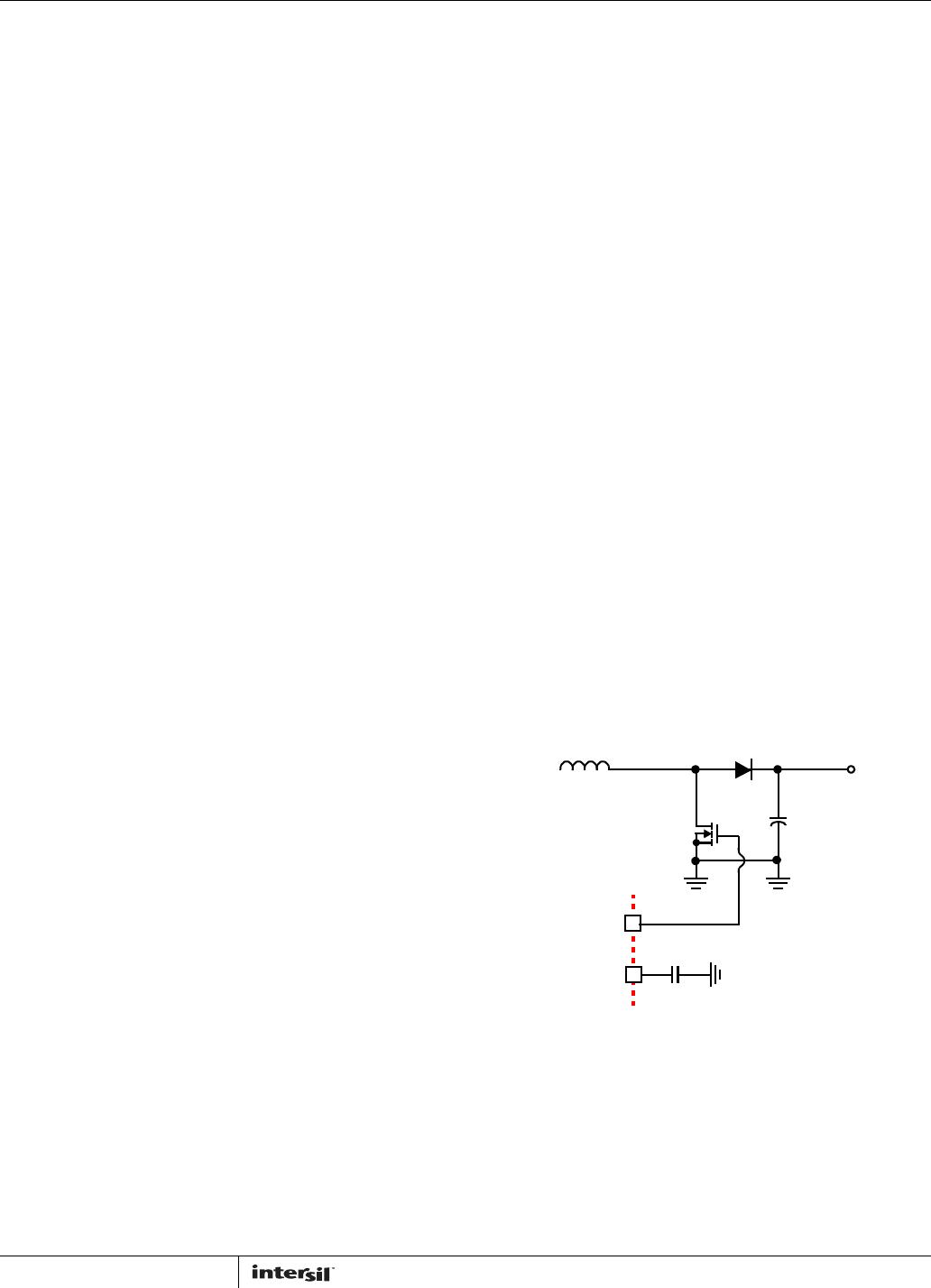
Figure 14 shows the critical power components; Q
1
, D and C
OUT
.
To minimize the voltage overshoot, the interconnecting wires
indicated by heavy lines should be part of the ground or the
power plane in a printed circuit board. The components shown in
Figure 14 should be located as close together as possible. Please
note that the capacitors C
VCC
and C
O
each represent numerous
physical capacitors. Locate the ISL6730A, ISL6730B, ISL6730C,
ISL6730D within 2 inches of the MOSFET, Q
1
. The circuit traces
for the MOSFETs’ gate and source connections from the
ISL6730A, ISL6730B, ISL6730C, ISL6730D must be sized to
handle up to 1.5A peak current.
Component Selection Guidelines
A 300W, universal input, PFC converter design is provided for
demonstration. The design method is for a continuous current
mode power factor correction boost converter with the
ISL6730B/D. The switching frequency is 62kHz.
C
BO
0.22μF»
(EQ. 6)
FIGURE 14. CRITICAL CURRENT POWER COMPONENTS
Q
1
C
OUT
L
D
GATE
VCC
C
VCC

ISL6730DFUZ

Mfr. #:
Manufacturer:
Renesas / Intersil
Description:
Power Factor Correction - PFC PFC Controller
Lifecycle:
New from this manufacturer.
Delivery:
DHL FedEx Ups TNT EMS
Payment:
T/T Paypal Visa MoneyGram Western Union