ISL6730A, ISL6730B, ISL6730C, ISL6730D
16
FN8258.1
August 8, 2013
INPUT VOLTAGE SETTING
First, set the BO resistor divider gain, K
BO
according to
Equations 1 and 2.
Assuming the converter starts at V
LINE
= 80V
RMS
, then the BO
resistor divider gain, K
BO
should be:
In this design, two 3.3MΩ resistors in series are used for R
IN2
.
So, R
IN1
is calculated:
Using resistor from the standard value, R
IN1
= 43kΩ, the actual
K
BO
is calculated:
NEGATIVE INPUT CAPACITOR GENERATION
The ISL6730A, ISL6730B, ISL6730C, ISL6730D generates an
equivalent negative capacitance at the input to cancel the input
filter capacitance. Thus, more input capacitors can be used
without reducing the power factor.
The input equivalent negative capacitance is a function of the
current sensing gain, BO resistor divider gain and the
compensation components.
This equivalent negative capacitor cancels the input filter
capacitor required for EMI filtering. Therefore, the displacement
power factor significantly improves.
For example, C
F2
= 0.68µF, C
F1
= 0.94µF, using the low cost EMI
filter shown in Figure 13. When V
LINE
= 230VAC, f
LINE
= 50Hz,
P
O
= 60W.
Assuming 95% efficiency under the above test condition, the
resistive component, which is in phase to voltage:
The reactive current through the input capacitors:
Thus, the displacement power factor is:
The reactive current generated by the equivalent negative
capacitor is:
With the equivalent negative capacitor, the total reactive current
reduces to:
The displacement power factor increases to:
VOLTAGE LOOP COMPENSATION
The average diode forward current can be approximated by:
Assuming the input current traces the input voltage perfectly. The
input power is in proportion to (V
COMP
- 1V).
Where Δ
COMP
is the V
COMP
- 1V. 1V is the offset voltage.
R
IS
is the internal current scaling resistor. R
IS
= 14.2kΩ.
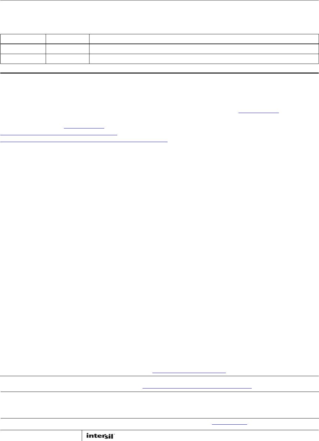
FIGURE 17. BODE PLOT OF THE ACTUAL CURRENT LOOP GAIN
-20
0
20
40
60
80
GAIN (dB)
10 100
1x10
3
0
45
90
135
180
FREQUENCY (Hz)
PHASE (°)
45
60
10.5kHz
1x10
3
1x10
3
10.5kHz
K
BO
0.5V
80V 2V–
------------------------
0.00641==
(EQ. 57)
R
IN1
0.00641
1 0.00641–
------------------------------ -
6.6MΩ()⋅ 42.6kΩ==
(EQ. 58)
K
BO
R
IN1
R
IN1
R
IN2
+
---------------------------------
0.00647==
(EQ. 59)
C
NEG
K
BO
0.8
V
m
V
OUT
----------------
–⋅
⎝⎠
⎜⎟
⎛⎞
R
SEN
R
CS
A
iDC
--------------------------
C
ic
C
ip
+()=
(EQ. 60)
C
NEG
0.00647 0.8
1.5
390
--------- -
–⋅
⎝⎠
⎛⎞
3.16k
0.068 1.9⋅
---------------------------
18nF 1.2nF+()= 0.62μF=
(EQ. 61)
I
a
P
o
V
LINE
0.95⋅
---------------------------------
= 0.275A=
(EQ. 62)
I
c
V
LINE
2π f
LINE
⋅()• C
F1
C
F2
+()•= 0.117A=
(EQ. 63)
PF
DIS
I
a
I
a
()
2
I
c
()
2
+
-----------------------------------
= 0.92=
(EQ. 64)
I
cneg
V
LINE
2π f
LINE
⋅()• C
NEG
()•= 0.045A=
(EQ. 65)
I
c
I
cneg
– 0.072A=
(EQ. 66)
PF
DIS
I
a
I
a
()
2
I
c
I
cneg
–()
2
+
--------------------------------------------------------
= 0.967=
(EQ. 67)
I
Dave()
P
in
V
OUT
----------------
=
(EQ. 68)
I
Dave()
R
SEN
R
CS
0.5 R⋅
IS
⋅
---------------------------------------
1
V
OUT
----------------
•
0.25
22()π⁄()
2
K
BO
⋅
------------------------------------------------
⎝⎠
⎜⎟
⎜⎟
⎛⎞
Δ
COMP
••=
(EQ. 69)
I
Dave()
0.598
A
V
--- -
Δ
COMP
•=
(EQ. 70)