XC2C128 CoolRunner-II CPLD
DS093 (v3.2) March 8, 2007 www.xilinx.com 7
Product Specification
R
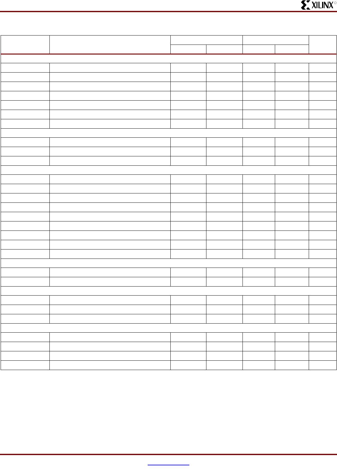
AC Electrical Characteristics Over Recommended Operating Conditions
Symbol Parameter
-6 -7
UnitsMin. Max. Min. Max.
T
PD1
Propagation delay single p-term - 5.7 - 7.0 ns
T
PD2
Propagation delay OR array - 6.0 - 7.5 ns
T
SUD
Direct input register set-up time 3.6 - 4.6 - ns
T
SU1
Setup time fast (single p-term) 2.4 - 3.0 - ns
T
SU2
Setup time (OR array) 2.7 - 3.5 - ns
T
HD
Direct input register hold time 0.0 - 0.0 - ns
T
H
Hold time (Or array or p-term) 0.0 - 0.0 - ns
T
CO
Clock to output - 4.2 - 5.4 ns
F
TOGGLE
(1)
Internal toggle rate - 450 - 300 MHz
F
SYSTEM1
(2)
Maximum system frequency - 244 - 152 MHz
F
SYSTEM2
(2)
Maximum system frequency - 227 - 141 MHz
F
EXT1
(3)
Maximum external frequency - 152 - 119 MHz
F
EXT2
(3)
Maximum external frequency - 145 - 112 MHz
T
PSUD
Direct input register p-term clock setup time 2.5 - 3.1 - ns
T
PSU1
P-term clock setup time (single p-term) 1.3 - 1.5 - ns
T
PSU2
P-term clock setup time (OR array) 1.6 - 2.0 - ns
T
PHD
Direct input register p-term clock hold time 0.2 - 0.2 - ns
T
PH
P-term clock hold 0.7 - 1.0 - ns
T
PCO
P-term clock to output - 5.9 - 7.3 ns
T
OE
/T
OD
Global OE to output enable/disable - 5.9 - 7.5 ns
T
POE
/T
POD
P-term OE to output enable/disable - 7.0 - 8.5 ns
T
MOE
/T
MOD
Macrocell driven OE to output enable/disable - 7.7 - 9.9 ns
T
PAO
P-term set/reset to output valid - 6.6 - 8.1 ns
T
AO
Global set/reset to output valid - 5.0 - 7.6 ns
T
SUEC
Register clock enable setup time 3.1 - 3.5 - ns
T
HEC
Register clock enable hold time 0.0 - 0.0 - ns
T
CW
Global clock pulse width High or Low 1.1 - 1.6 - ns
T
APRPW
Asynchronous preset/reset pulse width (High or Low) 6.0 - 7.5 - ns
T
PCW
P-term pulse width High or Low 6.0 - 7.5 - ns
T
DGSU
Set-up before DataGATE latch assertion 0.0 - 0.0 - ns
T
DGH
Hold to DataGATE latch assertion 4.0 - 6.0 - ns
T
DGR
DataGATE recovery to new data - 8.2 - 9.0 ns
T
DGW
DataGATE low pulse width 3.0 - 4.0 - ns
T
CDRSU
CDRST setup time before falling edge GCLK2 1.3 - 2.0 - ns
T
CDRH
Hold time CDRST after falling edge GCLK2 0.0 - 0.0 - ns
T
CONFIG
(4)
Configuration time - 350 - 350 us
Notes:
1. F
TOGGLE
is the maximum clock frequency to which a T flip-flop can reliably toggle (see the CoolRunner-II family data sheet).
2. F
SYSTEM1
is the internal operating frequency for a device with 16-bit resetable binary counter through one p-term per macrocell while
F
SYSTEM2
is through the OR array (one counter per function block).
3. F
EXT1
(1/T
SU1
+T
CO
) is the maximum external frequency using one p-term while F
EXT2
is through the OR array.
4. Typical configuration current during
T
CONFIG
is 10 mA.
XC2C128 CoolRunner-II CPLD
8 www.xilinx.com DS093 (v3.2) March 8, 2007
Product Specification
R
Internal Timing Parameters
Symbol Parameter
(1)
-6 -7
UnitsMin. Max. Min. Max.
Buffer Delays
T
IN
Input buffer delay - 2.0 - 2.6 ns
T
DIN
Direct data register input delay - 3.7 - 5.3 ns
T
GCK
Global Clock buffer delay - 1.5 - 2.1 ns
T
GSR
Global set/reset buffer delay - 1.6 - 3.5 ns
T
GTS
Global 3-state buffer delay - 2.1 - 3.0 ns
T
OUT
Output buffer delay - 2.3 - 2.6 ns
T
EN
Output buffer enable/disable delay - 3.8 - 4.5 ns
P-term Delays
T
CT
Control term delay - 1.2 - 1.4 ns
T
LOGI1
Single P-term delay adder - 0.5 - 1.1 ns
T
LOGI2
Multiple P-term delay adder - 0.3 - 0.5 ns
Macrocell Delay
T
PDI
Input to output valid - 0.9 - 0.7 ns
T
LDI
Setup before clock (transparent latch) - 2.1 - 2.5 ns
T
SUI
Setup before clock 1.4 - 1.4 - ns
T
HI
Hold after clock 0.0 - 0.0 - ns
T
ECSU
Enable clock setup time 1.4 - 1.6 - ns
T
ECHO
Enable clock hold time 0.0 - 0.0 - ns
T
COI
Clock to output valid - 0.4 - 0.7 ns
T
AOI
Set/reset to output valid - 1.1 - 1.5 ns
T
CDBL
Clock doubler delay - 0.0 - 0.0 ns
Feedback Delays
T
F
Feedback delay - 1.8 - 3.4 ns
T
OEM
Macrocell to global OE delay - 2.0 - 2.6 ns
I/O Standard Time Adder Delays 1.5V CMOS
T
HYS15
Hysteresis input adder - 3.0 - 4.0 ns
T
OUT15
Output adder - 0.8 - 1.0 ns
T
SLEW15
Output slew rate adder - 4.0 - 4.0 ns
I/O Standard Time Adder Delays 1.8V CMOS
T
HYS18
Hysteresis input adder - 2.0 - 4.0 ns
T
IN18
Input adder - 0 - 0 ns
T
OUT18
Output adder - 0.0 - 0.0 ns
T
SLEW18
Output slew rate adder - 2.5 - 4.0 ns
XC2C128 CoolRunner-II CPLD
DS093 (v3.2) March 8, 2007 www.xilinx.com 9
Product Specification
R
Switching Characteristics
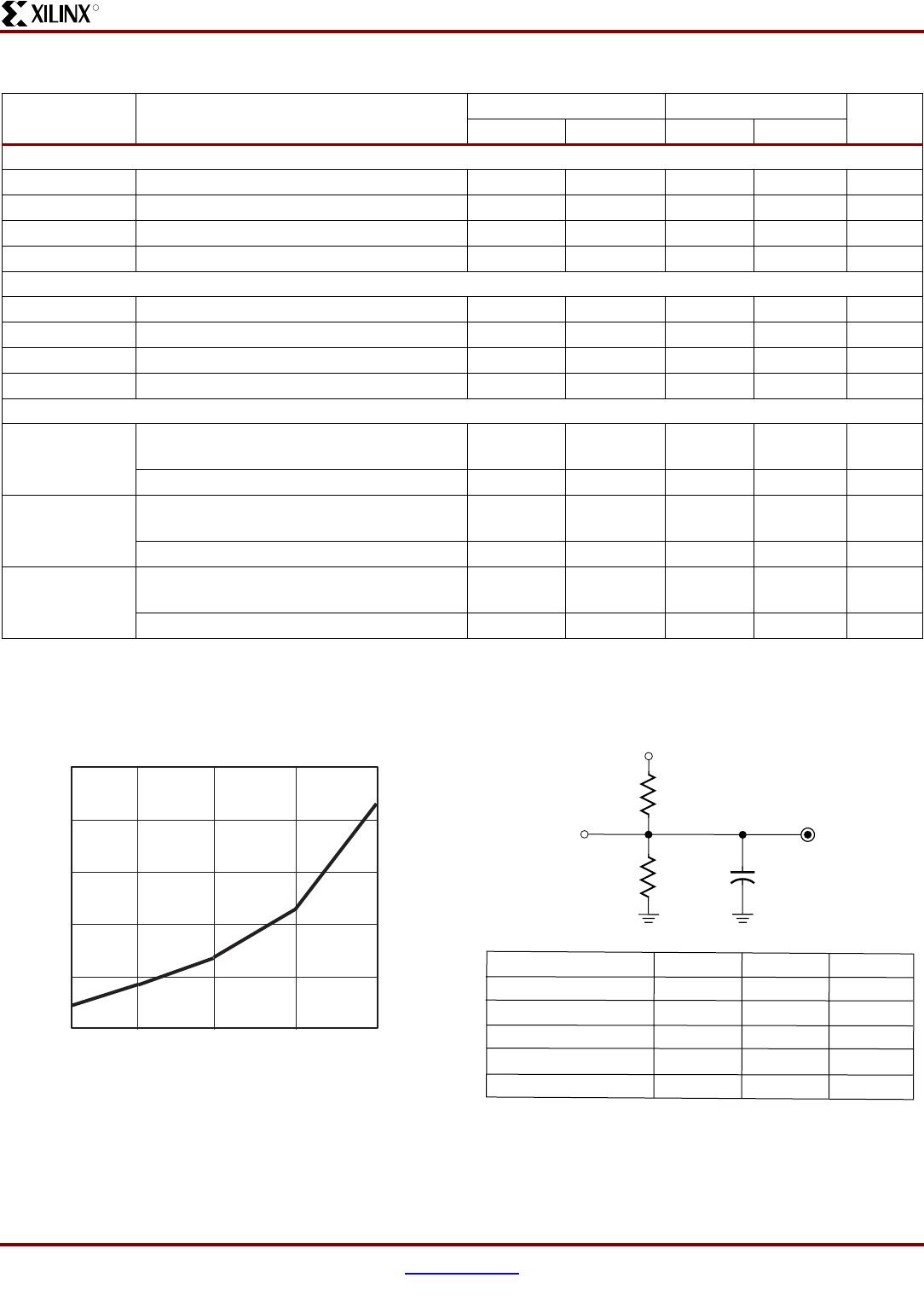
Figure 2: Derating Curve for T
PD
Switching Test Conditions
Figure 3: AC Load Circuits
I/O Standard Time Adder Delays 2.5V CMOS
T
IN25
Standard input adder - 0.6 - 0.7 ns
T
HYS25
Hysteresis input adder - 1.5 - 3.0 ns
T
OUT25
Output adder - 0.8 - 0.9 ns
T
SLEW25
Output slew rate adder - 3.0 - 4.0 ns
I/O Standard Time Adder Delays 3.3V CMOS/TTL
T
IN33
Standard input adder - 0.5 - 0.6 ns
T
HYS33
Hysteresis input adder - 1.2 - 3.0 ns
T
OUT33
Output adder - 1.2 - 1.4 ns
T
SLEW33
Output slew rate adder - 3.0 - 4.0 ns
I/O Standard Time Adder Delays HSTL, SSTL
SSTL2-1 Input adder to T
IN
, T
DIN
, T
GCK
, T
GSR
,
T
GTS
- 0.8 - 2.5 ns
Output adder to T
OUT
- 0.5 - 0.5 ns
SSTL3-1 Input adder to T
IN
, T
DIN
, T
GCK
, T
GSR
,
T
GTS
- 0.8 - 2.5 ns
Output adder to T
OUT
- 0.5 - 0.5 ns
HSTL-1 Input adder to T
IN
, T
DIN
, T
GCK
, T
GSR
,
T
GTS
- 2.0 - 2.5 ns
Output adder to T
OUT
- 0.0 - 0.0 ns
Notes:
1. 1.5 ns input pin signal rise/fall.
Internal Timing Parameters (Continued)
Symbol Parameter
(1)
-6 -7
UnitsMin. Max. Min. Max.
Number of Outputs Switching
12 4 8 16
4.0
4.4
4.8
V
CC
= V
CCIO
= 1.8V, 25
o
C
T
PD2
(ns)
5.0
4.6
4.2
DS093_02_050103
R
1
V
CC
C
L
R
2
Device
Under Test
Output Type
LVTTL33
LVCMOS33
LVCMOS25
LVCMOS18
LVCMOS15
R
1
268Ω
275Ω
188Ω
112.5Ω
150Ω
R
2
235Ω
275Ω
188Ω
112.5Ω
150Ω
C
L
35 pF
35 pF
35 pF
35 pF
35 pF
DS092_03_092302
Test Point
Notes:
1. C
L
includes test fixtures and probe capacitance.
2. 1.5 nsec maximum rise/fall times on inputs.

XC2C128-7CPG132C

Mfr. #:
Manufacturer:
Xilinx
Description:
CPLD - Complex Programmable Logic Devices XC2C128-7CPG132C
Lifecycle:
New from this manufacturer.
Delivery:
DHL FedEx Ups TNT EMS
Payment:
T/T Paypal Visa MoneyGram Western Union