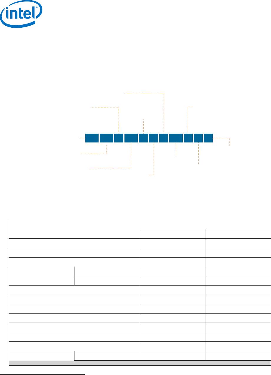
Resource Member Code
D5 D6
Receiver 72 72
PCIe Hard IP Block 2 2
FPGA Hard Memory Controller 1 1
HPS Hard Memory Controller 1 1
Arm Cortex-A9 MPCore Processor Dual-core Dual-core
Related Information
True LVDS Buffers in Devices, I/O Features in Cyclone V Devices
Provides the number of LVDS channels in each device package.
Package Plan
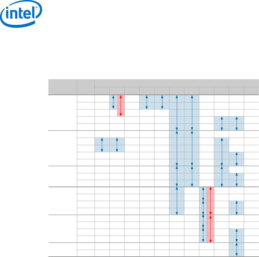
Table 15. Package Plan for Cyclone V ST Devices
• The HPS I/O counts are the number of I/Os in the HPS and does not correlate with the number of HPS-
specific I/O pins in the FPGA. Each HPS-specific pin in the FPGA may be mapped to several HPS I/Os.
• Transceiver counts shown are for transceiver ≤5 Gbps . 6 Gbps transceiver channel count support depends
on the package and channel usage. For more information about the 6 Gbps transceiver channel count,
refer to the Cyclone V Device Handbook Volume 2: Transceivers.
Member Code F896
(31 mm)
FPGA GPIO HPS I/O XCVR
D5 288 181 9
(11)
D6 288 181 9
(11)
Related Information
6.144-Gbps Support Capability in Cyclone V GT Devices, Cyclone V Device Handbook
Volume 2: Transceivers
Provides more information about 6 Gbps transceiver channel count.
(11)
If you require CPRI (at 4.9152 Gbps) and PCIe Gen2 transmit jitter compliance, Intel
recommends that you use only up to seven full-duplex transceiver channels for CPRI, and up
to six full-duplex channels for PCIe Gen2. The CMU channels are not considered full-duplex
channels.
Cyclone V Device Overview
CV-51001 | 2018.05.07
Cyclone V Device Overview
17