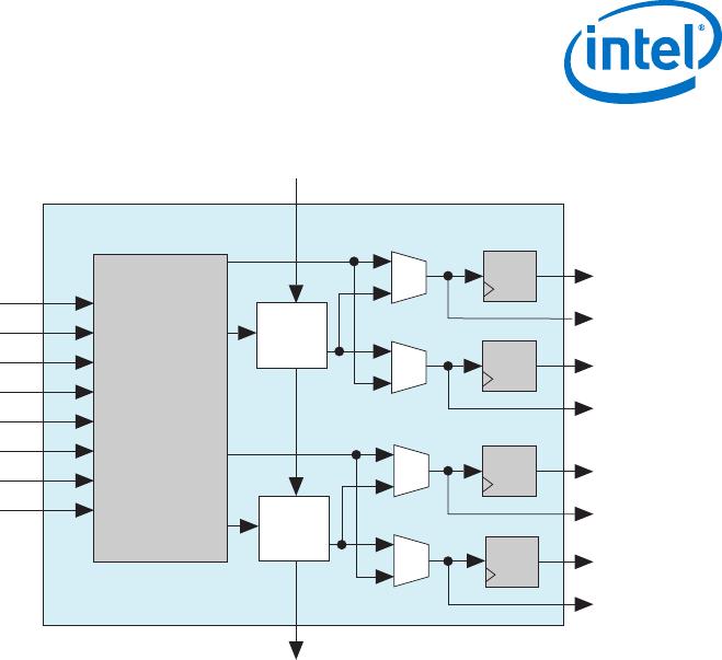
Variant Member
Code
Variable-
precision
DSP Block
Independent Input and Output
Multiplications Operator
18 x 18
Multiplier
Adder Mode
18 x 18
Multiplier
Adder
Summed
with 36 bit
Input
9 x 9
Multiplier
18 x 18
Multiplier
27 x 27
Multiplier
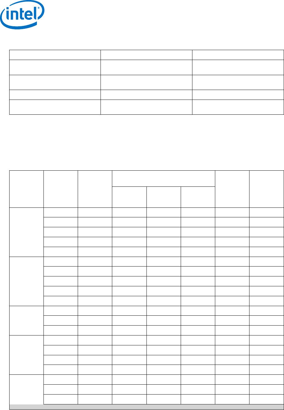
C6 112 336 224 112 112 112
Cyclone V ST D5 87 261 174 87 87 87
D6 112 336 224 112 112 112
Embedded Memory Blocks
The embedded memory blocks in the devices are flexible and designed to provide an
optimal amount of small- and large-sized memory arrays to fit your design
requirements.
Types of Embedded Memory
The Cyclone V devices contain two types of memory blocks:
• 10 Kb M10K blocks—blocks of dedicated memory resources. The M10K blocks are
ideal for larger memory arrays while still providing a large number of independent
ports.
• 640 bit memory logic array blocks (MLABs)—enhanced memory blocks that are
configured from dual-purpose logic array blocks (LABs). The MLABs are ideal for
wide and shallow memory arrays. The MLABs are optimized for implementation of
shift registers for digital signal processing (DSP) applications, wide shallow FIFO
buffers, and filter delay lines. Each MLAB is made up of ten adaptive logic modules
(ALMs). In the Cyclone V devices, you can configure these ALMs as ten 32 x 2
blocks, giving you one 32 x 20 simple dual-port SRAM block per MLAB.
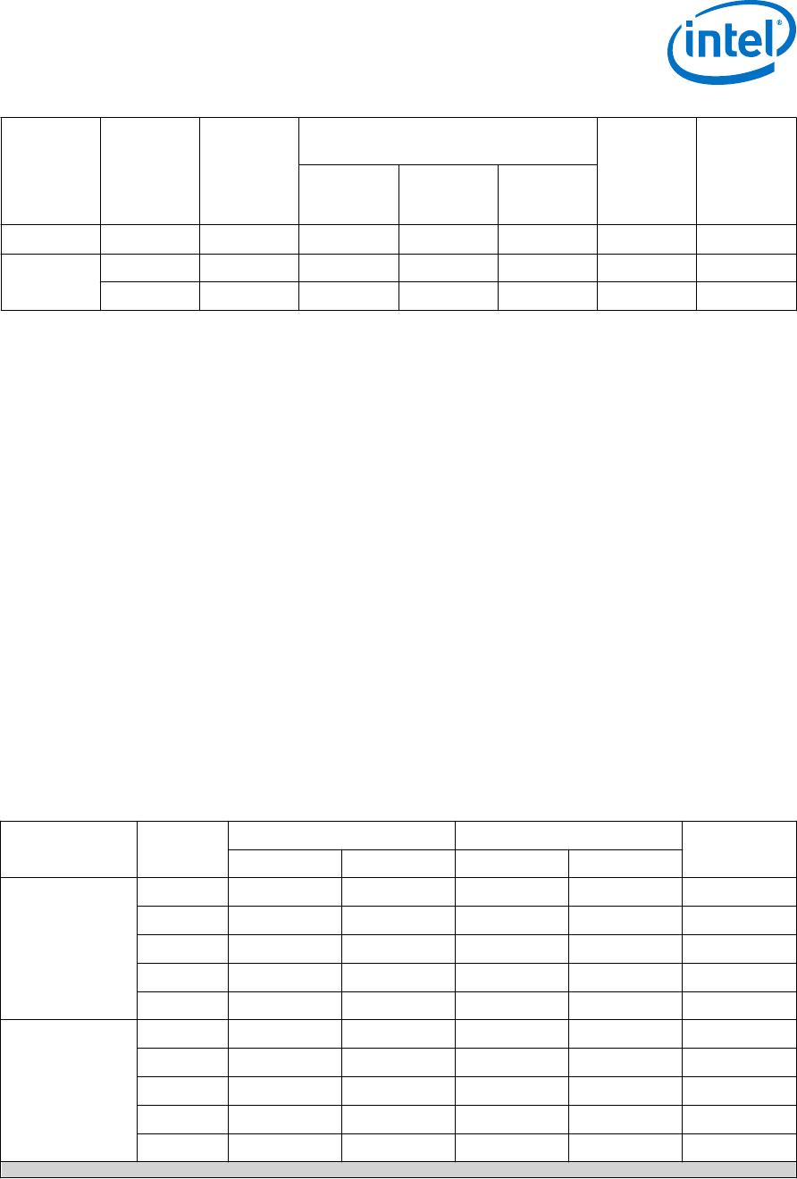
Embedded Memory Capacity in Cyclone V Devices
Table 18. Embedded Memory Capacity and Distribution in Cyclone V Devices
Variant
Member
Code
M10K MLAB
Total RAM Bit
(Kb)Block RAM Bit (Kb) Block RAM Bit (Kb)
Cyclone V E A2 176 1,760 314 196 1,956
A4 308 3,080 485 303 3,383
A5 446 4,460 679 424 4,884
A7 686 6,860 1338 836 7,696
A9 1,220 12,200 2748 1,717 13,917
Cyclone V GX C3 135 1,350 291 182 1,532
C4 250 2,500 678 424 2,924
C5 446 4,460 678 424 4,884
C7 686 6,860 1338 836 7,696
C9 1,220 12,200 2748 1,717 13,917
continued...
Cyclone V Device Overview
CV-51001 | 2018.05.07
Cyclone V Device Overview
21