PCS Support Data Rates
(Gbps)
Transmitter Data Path Feature Receiver Data Path Feature
Serial ATA Gen1 and Gen2 1.5 and 3.0 Custom PHY IP core with preset
feature
Electrical idle
Custom PHY IP core with preset
feature
Signal detect
Wider spread of asynchronous
SSC
CPRI 4.1
(16)
0.6144 to 6.144 Dedicated deterministic latency
PHY IP core
Transmitter (TX) manual bit-slip
mode
Dedicated deterministic latency
PHY IP core
Receiver (RX) deterministic
latency state machine
OBSAI RP3 0.768 to 3.072
V-by-One HS Up to 3.75 Custom PHY IP core Custom PHY IP core
Wider spread of asynchronous
SSC
DisplayPort 1.2
(17)
1.62 and 2.7
SoC with HPS
Each SoC combines an FPGA fabric and an HPS in a single device. This combination
delivers the flexibility of programmable logic with the power and cost savings of hard
IP in these ways:
Reduces board space, system power, and bill of materials cost by eliminating a
discrete embedded processor
Allows you to differentiate the end product in both hardware and software, and to
support virtually any interface standard
Extends the product life and revenue through in-field hardware and software
updates
HPS Features
The HPS consists of a dual-core Arm Cortex-A9 MPCore processor, a rich set of
peripherals, and a shared multiport SDRAM memory controller, as shown in the
following figure.
(16)
High-voltage output mode (1000-BASE-CX) is not supported.
(17)
Pending characterization.
Cyclone V Device Overview
CV-51001 | 2018.05.07
Cyclone V Device Overview
28
Figure 11. HPS with Dual-Core Arm Cortex-A9 MPCore Processor
FPGA Fabric
HPS
HPS-to-FPGA
Lightweight
HPS-to-FPGA
FPGA-to-HPS
FPGA-to-HPS SDRAM
Configuration
Controller
FPGA
Manager
64 KB
On-Chip RAM
64 KB
Boot ROM
Level 3
Interconnect
Ethernet
MAC (2x)
USB
OTG (2x)
NAND Flash
Controller
SD/MMC
Controller
DMA
Controller
STM
ETR
(Trace)
Debug
Access Port
ARM Cortex-A9 MPCore
MPU Subsystem
CPU0
ARM Cortex-A9
with NEON/FPU,
32 KB Instruction Cache,
32 KB Data Cache, and
Memory Management
Unit
CPU1
ARM Cortex-A9
with NEON/FPU,
32 KB Instruction Cache,
32 KB Data Cache, and
Memory Management
Unit
SCUACP
Level 2 Cache (512 KB)
Multiport
DDR SDRAM
Controller
with
Optional ECC
Peripherals
(UART, Timer, I
2
C, Watchdog Timer, GPIO, SPI, Clock Manager, Reset Manager, Scan Manager, System Manager, and Quad
SPI Flash Controller)
System Peripherals and Debug Access Port
Each Ethernet MAC, USB OTG, NAND flash controller, and SD/MMC controller module
has an integrated DMA controller. For modules without an integrated DMA controller,
an additional DMA controller module provides up to eight channels of high-bandwidth
data transfers. Peripherals that communicate off-chip are multiplexed with other
peripherals at the HPS pin level. This allows you to choose which peripherals to
interface with other devices on your PCB.
The debug access port provides interfaces to industry standard JTAG debug probes
and supports Arm CoreSight debug and core traces to facilitate software development.
Cyclone V Device Overview
CV-51001 | 2018.05.07
Cyclone V Device Overview
29
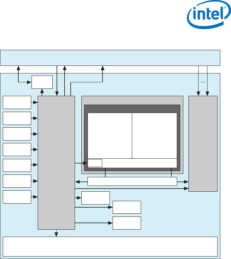
HPS–FPGA AXI Bridges
The HPS–FPGA bridges, which support the Advanced Microcontroller Bus Architecture
(AMBA
®
) Advanced eXtensible Interface (AXI
) specifications, consist of the following
bridges:
FPGA-to-HPS AXI bridge—a high-performance bus supporting 32, 64, and 128 bit
data widths that allows the FPGA fabric to issue transactions to slaves in the HPS.
HPS-to-FPGA AXI bridge—a high-performance bus supporting 32, 64, and 128 bit
data widths that allows the HPS to issue transactions to slaves in the FPGA fabric.
Lightweight HPS-to-FPGA AXI bridge—a lower latency 32 bit width bus that allows
the HPS to issue transactions to slaves in the FPGA fabric. This bridge is primarily
used for control and status register (CSR) accesses to peripherals in the FPGA
fabric.
The HPS–FPGA AXI bridges allow masters in the FPGA fabric to communicate with
slaves in the HPS logic, and vice versa. For example, the HPS-to-FPGA AXI bridge
allows you to share memories instantiated in the FPGA fabric with one or both
microprocessors in the HPS, while the FPGA-to-HPS AXI bridge allows logic in the
FPGA fabric to access the memory and peripherals in the HPS.
Each HPS–FPGA bridge also provides asynchronous clock crossing for data transferred
between the FPGA fabric and the HPS.
HPS SDRAM Controller Subsystem
The HPS SDRAM controller subsystem contains a multiport SDRAM controller and DDR
PHY that are shared between the FPGA fabric (through the FPGA-to-HPS SDRAM
interface), the level 2 (L2) cache, and the level 3 (L3) system interconnect. The
FPGA-to-HPS SDRAM interface supports AMBA AXI and Avalon
®
Memory-Mapped
(Avalon-MM) interface standards, and provides up to six individual ports for access by
masters implemented in the FPGA fabric.
To maximize memory performance, the SDRAM controller subsystem supports
command and data reordering, deficit round-robin arbitration with aging, and
high-priority bypass features. The SDRAM controller subsystem supports DDR2, DDR3,
or LPDDR2 devices up to 4 Gb in density operating at up to 400 MHz (800 Mbps data
rate).
FPGA Configuration and Processor Booting
The FPGA fabric and HPS in the SoC are powered independently. You can reduce the
clock frequencies or gate the clocks to reduce dynamic power, or shut down the entire
FPGA fabric to reduce total system power.
You can configure the FPGA fabric and boot the HPS independently, in any order,
providing you with more design flexibility:
You can boot the HPS independently. After the HPS is running, the HPS can fully or
partially reconfigure the FPGA fabric at any time under software control. The HPS
can also configure other FPGAs on the board through the FPGA configuration
controller.
You can power up both the HPS and the FPGA fabric together, configure the FPGA
fabric first, and then boot the HPS from memory accessible to the FPGA fabric.
Cyclone V Device Overview
CV-51001 | 2018.05.07
Cyclone V Device Overview
30

5CGXFC7C6U19C7N

Mfr. #:
Manufacturer:
Intel / Altera
Description:
FPGA - Field Programmable Gate Array FPGA - Cyclone V GX 5648 LABs 224 IOs
Lifecycle:
New from this manufacturer.
Delivery:
DHL FedEx Ups TNT EMS
Payment:
T/T Paypal Visa MoneyGram Western Union