Summary of Cyclone V Features
Table 2. Summary of Features for Cyclone V Devices
Feature Description
Technology TSMC's 28-nm low-power (28LP) process technology
1.1 V core voltage
Packaging Wirebond low-halogen packages
Multiple device densities with compatible package footprints for seamless migration between
different device densities
RoHS-compliant and leaded
(1)
options
High-performance
FPGA fabric
Enhanced 8-input ALM with four registers
Internal memory
blocks
M10K—10-kilobits (Kb) memory blocks with soft error correction code (ECC)
Memory logic array block (MLAB)—640-bit distributed LUTRAM where you can use up to 25%
of the ALMs as MLAB memory
Embedded Hard IP
blocks
Variable-precision DSP Native support for up to three signal processing precision levels
(three 9 x 9, two 18 x 18, or one 27 x 27 multiplier) in the same
variable-precision DSP block
64-bit accumulator and cascade
Embedded internal coefficient memory
Preadder/subtractor for improved efficiency
Memory controller DDR3, DDR2, and LPDDR2 with 16 and 32 bit ECC support
Embedded transceiver
I/O
PCI Express* (PCIe*) Gen2 and Gen1 (x1, x2, or x4) hard IP with
multifunction support, endpoint, and root port
Clock networks Up to 550 MHz global clock network
Global, quadrant, and peripheral clock networks
Clock networks that are not used can be powered down to reduce dynamic power
Phase-locked loops
(PLLs)
Precision clock synthesis, clock delay compensation, and zero delay buffering (ZDB)
Integer mode and fractional mode
FPGA General-purpose
I/Os (GPIOs)
875 megabits per second (Mbps) LVDS receiver and 840 Mbps LVDS transmitter
400 MHz/800 Mbps external memory interface
On-chip termination (OCT)
3.3 V support with up to 16 mA drive strength
Low-power high-speed
serial interface
614 Mbps to 6.144 Gbps integrated transceiver speed
Transmit pre-emphasis and receiver equalization
Dynamic partial reconfiguration of individual channels
HPS
(Cyclone V SE, SX,
and ST devices only)
Single or dual-core Arm Cortex-A9 MPCore processor-up to 925 MHz maximum frequency with
support for symmetric and asymmetric multiprocessing
Interface peripherals—10/100/1000 Ethernet media access control (EMAC), USB 2.0
On-The-GO (OTG) controller, quad serial peripheral interface (QSPI) flash controller, NAND
flash controller, Secure Digital/MultiMediaCard (SD/MMC) controller, UART, controller area
network (CAN), serial peripheral interface (SPI), I
2
C interface, and up to 85 HPS GPIO
interfaces
System peripherals—general-purpose timers, watchdog timers, direct memory access (DMA)
controller, FPGA configuration manager, and clock and reset managers
On-chip RAM and boot ROM
continued...
(1)
Contact Intel for availability.
Cyclone V Device Overview
CV-51001 | 2018.05.07
Cyclone V Device Overview
4
Feature Description
HPS–FPGA bridges—include the FPGA-to-HPS, HPS-to-FPGA, and lightweight HPS-to-FPGA
bridges that allow the FPGA fabric to issue transactions to slaves in the HPS, and vice versa
FPGA-to-HPS SDRAM controller subsystem—provides a configurable interface to the multiport
front end (MPFE) of the HPS SDRAM controller
Arm CoreSight
JTAG debug access port, trace port, and on-chip trace storage
Configuration Tamper protection—comprehensive design protection to protect your valuable IP investments
Enhanced advanced encryption standard (AES) design security features
CvP
Dynamic reconfiguration of the FPGA
Active serial (AS) x1 and x4, passive serial (PS), JTAG, and fast passive parallel (FPP) x8 and
x16 configuration options
Internal scrubbing
(2)
Partial reconfiguration
(3)
Cyclone V Device Variants and Packages
Table 3. Device Variants for the Cyclone V Device Family
Variant Description
Cyclone V E Optimized for the lowest system cost and power requirement for a wide spectrum of general logic
and DSP applications
Cyclone V GX Optimized for the lowest cost and power requirement for 614 Mbps to 3.125 Gbps transceiver
applications
Cyclone V GT The FPGA industry’s lowest cost and lowest power requirement for 6.144 Gbps transceiver
applications
Cyclone V SE SoC with integrated Arm-based HPS
Cyclone V SX SoC with integrated Arm-based HPS and 3.125 Gbps transceivers
Cyclone V ST SoC with integrated Arm-based HPS and 6.144 Gbps transceivers
Cyclone V E
This section provides the available options, maximum resource counts, and package
plan for the Cyclone V E devices.
The information in this section is correct at the time of publication. For the latest
information and to get more details, refer to the Product Selector Guide.
Related Information
Product Selector Guide
Provides the latest information about Intel products.
(2)
The SEU internal scrubbing feature is available for Cyclone V E, GX, SE, and SX devices with
the "SC" suffix in the part number. For device availability and ordering, contact your local Intel
sales representatives.
(3)
The partial reconfiguration feature is available for Cyclone V E, GX, SE, and SX devices with
the "SC" suffix in the part number. For device availability and ordering, contact your local
Intel
®
sales representatives.
Cyclone V Device Overview
CV-51001 | 2018.05.07
Cyclone V Device Overview
5
Available Options
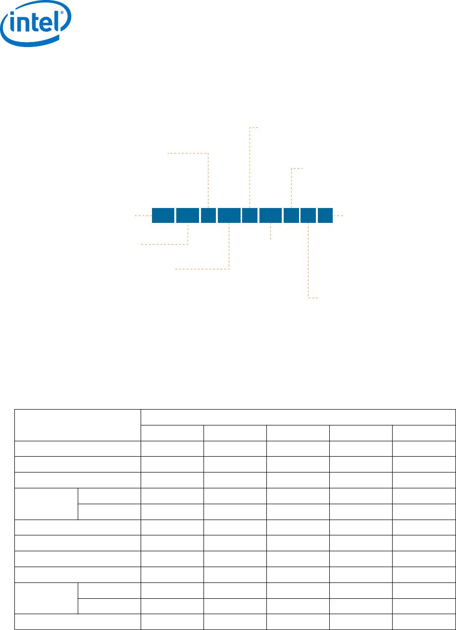
Figure 1. Sample Ordering Code and Available Options for Cyclone V E Devices
The SEU internal scrubbing feature is available for Cyclone V E, GX, SE, and SX devices with the "SC" suffix in
the part number. For device availability and ordering, contact your local Intel sales representatives.
Family Signature
Embedded Hard IPs
Package Type
Package Code
Operating Temperature
FPGA Fabric Speed Grade
Optional Suffix
Indicates specific device
options or shipment method
E : Enhanced logic/memory
B : No hard PCIe or hard
memory controller
F : No hard PCIe and maximum
2 hard memory controllers
5C : Cyclone V
F : FineLine BGA (FBGA)
U : Ultra FineLine BGA (UBGA)
M : Micro FineLine BGA (MBGA)
FBGA Package Type
17 : 256 pins
23 : 484 pins
27 : 672 pins
31 : 896 pins
UBGA Package Type
15 : 324 pins
19 : 484 pins
MBGA Package Type
13 : 383 pins
15 : 484 pins
C : Commercial (T
J
= 0° C to 85° C)
I : Industrial (T
J
= -40° C to 100° C)
A : Automotive (T
J
= -40° C to 125° C)
6 (fastest)
7
8
N : Lead-free packaging
Contact Intel for availability
of leaded options
ES : Engineering sample
5C
E F A9 F 31
C
7
N
Member Code
Family Variant
A2 : 25K logic elements
A4 : 49K logic elements
A5 : 77K logic elements
A7 : 150K logic elements
A9 : 301K logic elements
SC : Internal scrubbing support
Maximum Resources
Table 4. Maximum Resource Counts for Cyclone V E Devices
Resource Member Code
A2 A4 A5 A7 A9
Logic Elements (LE) (K) 25 49 77 150 301
ALM 9,430 18,480 29,080 56,480 113,560
Register 37,736 73,920 116,320 225,920 454,240
Memory (Kb) M10K 1,760 3,080 4,460 6,860 12,200
MLAB 196 303 424 836 1,717
Variable-precision DSP Block 25 66 150 156 342
18 x 18 Multiplier 50 132 300 312 684
PLL 4 4 6 7 8
GPIO 224 224 240 480 480
LVDS Transmitter 56 56 60 120 120
Receiver 56 56 60 120 120
Hard Memory Controller 1 1 2 2 2
Cyclone V Device Overview
CV-51001 | 2018.05.07
Cyclone V Device Overview
6

5CGXFC7C6U19C7N

Mfr. #:
Manufacturer:
Intel / Altera
Description:
FPGA - Field Programmable Gate Array FPGA - Cyclone V GX 5648 LABs 224 IOs
Lifecycle:
New from this manufacturer.
Delivery:
DHL FedEx Ups TNT EMS
Payment:
T/T Paypal Visa MoneyGram Western Union