Table 16: DDR3 I
DD
Specifications and Conditions – 8GB (Die Revisions E and J)
Values are for the MT41J512M8 DDR3 SDRAM only and are computed from values specified in the 4Gb (512 Meg x 8) com-
ponent data sheet
Parameter Symbol 1866 1600 1333 1066 Units
Operating current 0: One bank ACTIVATE-to-PRECHARGE I
DD0
1
640 584 520 496 mA
Operating current 1: One bank ACTIVATE-to-READ-to-PRECHARGE I
DD1
1
704 672 540 616 mA
Precharge power-down current: Slow exit I
DD2P0
2
288 288 288 288 mA
Precharge power-down current: Fast exit I
DD2P1
2
592 512 448 416 mA
Precharge quiet standby current I
DD2Q
2
560 512 448 416 mA
Precharge standby current I
DD2N
2
560 512 464 448 mA
Precharge standby ODT current I
DD2NT
2
480 456 424 400 mA
Active power-down current I
DD3P
2
656 608 560 512 mA
Active standby current I
DD3N
2
656 608 560 512 mA
Burst read operating current I
DD4R
1
1536 1400 1264 1128 mA
Burst write operating current I
DD4W
1
1272 1144 1024 904 mA
Refresh current I
DD5B
1
2080 2024 1968 1936 mA
Self refresh temperature current: MAX T
C
= 85°C I
DD6
2
320 320 320 320 mA
Self refresh temperature current (SRT-enabled): MAX T
C
= 95°C I
DD6ET
2
400 400 400 400 mA
All banks interleaved read current I
DD7
1
2152 1904 1664 1424 mA
Reset current I
DD8
2
320 320 320 320 mA
Notes:
1. One module rank in the active I
DD
; the other rank in I
DD2P0
(slow exit).
2. All ranks in this I
DD
condition.
2GB, 4GB, 8GB (x64, DR) 240-Pin DDR3 UDIMM
I
DD
Specifications
PDF: 09005aef837cdd2d
jtf16c256_512_1gx64az.pdf - Rev. I 04/13 EN
16
Micron Technology, Inc. reserves the right to change products or specifications without notice.
© 2008 Micron Technology, Inc. All rights reserved.
Serial Presence-Detect EEPROM
For the latest SPD data, refer to Micron's SPD page: www.micron.com/SPD.
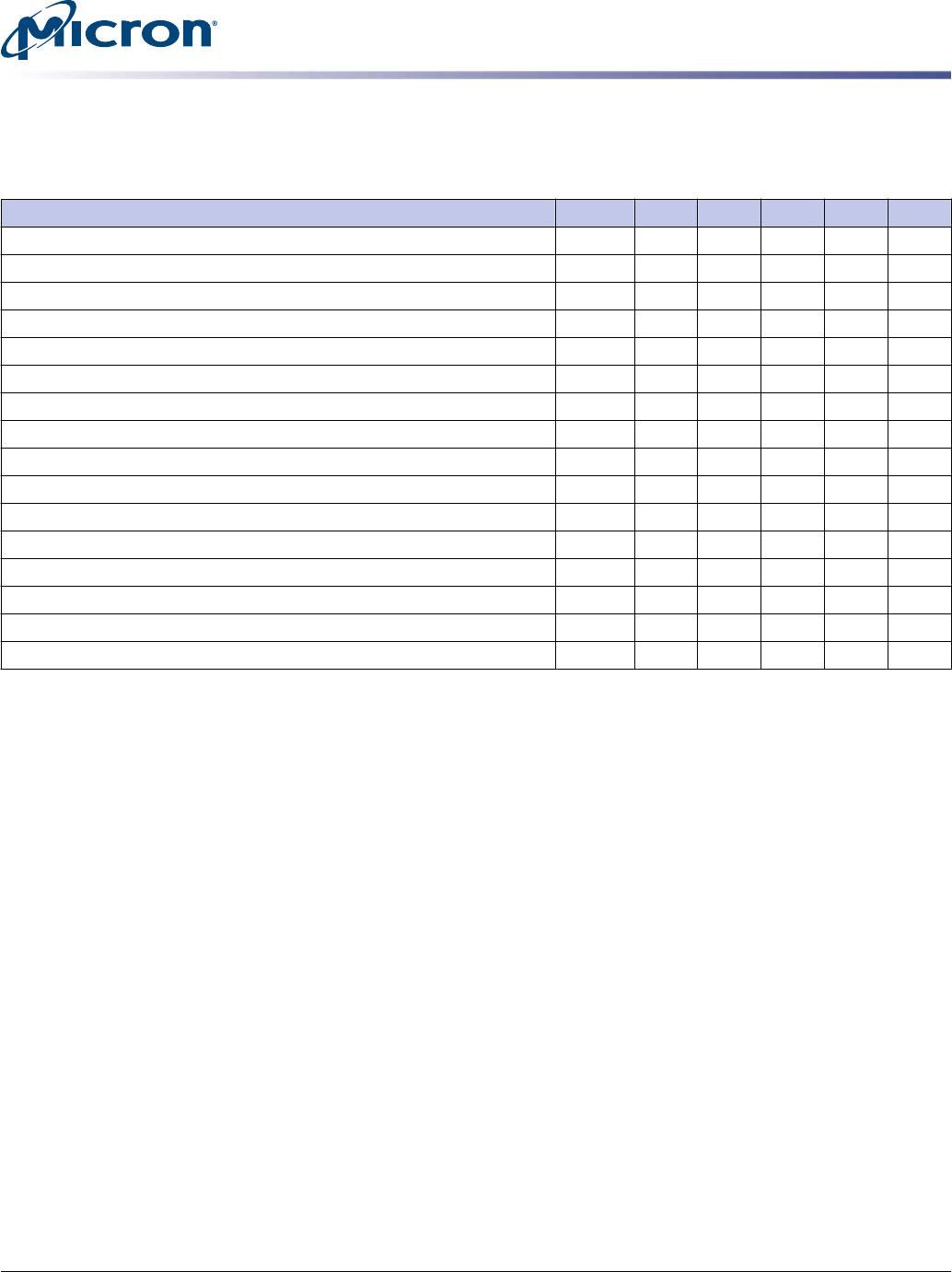
Table 17: Serial Presence-Detect EEPROM DC Operating Conditions
All voltages referenced to V
DDSPD
Parameter/Condition Symbol Min Max Units
Supply voltage V
DDSPD
3.0 3.6 V
Input low voltage: Logic 0; All inputs V
IL
–0.45 V
DDSPD
x 0.3 V
Input high voltage: Logic 1; All inputs V
IH
V
DDSPD
x 0.7 V
DDSPD
+ 1.0 V
Output low voltage: I
OUT
= 3mA V
OL
0.4 V
Input leakage current: V
IN
= GND to V
DD
I
LI
0.1 2.0 µA
Output leakage current: V
OUT
= GND to V
DD
I
LO
0.05 2.0 µA
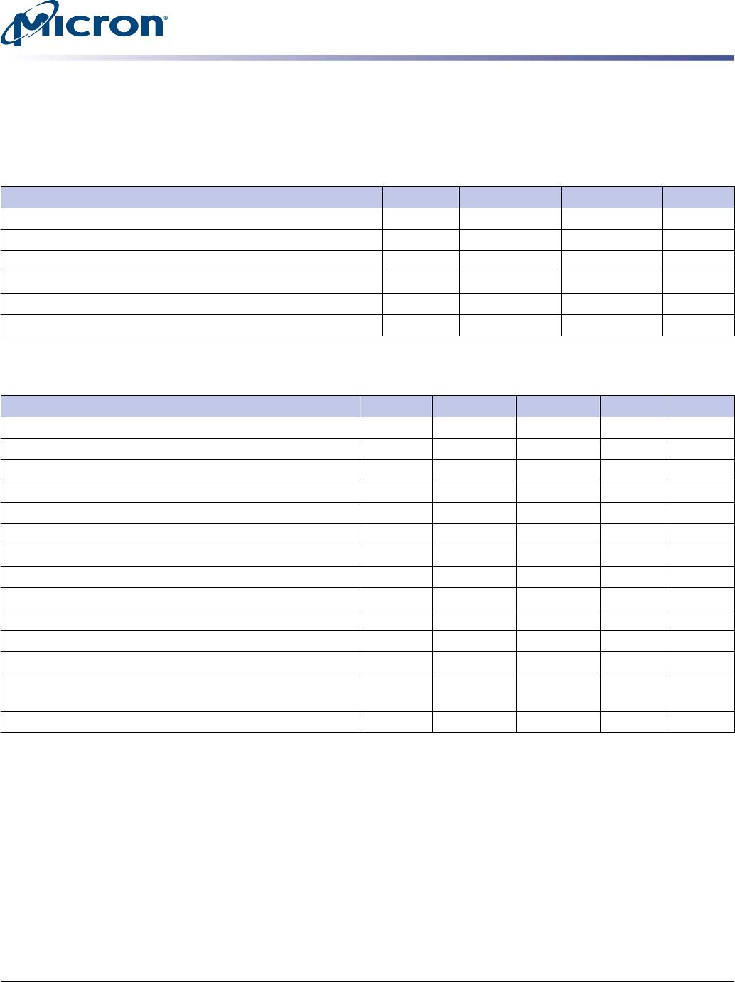
Table 18: Serial Presence-Detect EEPROM AC Operating Conditions
Parameter/Condition Symbol Min Max Units Notes
Clock frequency
t
SCL 10 400 kHz
Clock pulse width HIGH time
t
HIGH 0.6 µs
Clock pulse width LOW time
t
LOW 1.3 µs
SDA rise time
t
R 300 µs 1
SDA fall time
t
F 20 300 ns 1
Data-in setup time
t
SU:DAT 100 ns
Data-in hold time
t
HD:DI 0 µs
Data-out hold time
t
HD:DAT 200 900 ns
Data out access time from SCL LOW
t
AA:DAT 0.2 0.9 µs 2
Start condition setup time
t
SU:STA 0.6 µs 3
Start condition hold time
t
HD:STA 0.6 µs
Stop condition setup time
t
SU:STO 0.6 µs
Time the bus must be free before a new transition can
start
t
BUF 1.3 µs
WRITE time
t
W 10 ms
Notes:
1. Guaranteed by design and characterization, not necessarily tested.
2. To avoid spurious start and stop conditions, a minimum delay is placed between the fall-
ing edge of SCL and the falling or rising edge of SDA.
3. For a restart condition, or following a WRITE cycle.
2GB, 4GB, 8GB (x64, DR) 240-Pin DDR3 UDIMM
Serial Presence-Detect EEPROM
PDF: 09005aef837cdd2d
jtf16c256_512_1gx64az.pdf - Rev. I 04/13 EN
17
Micron Technology, Inc. reserves the right to change products or specifications without notice.
© 2008 Micron Technology, Inc. All rights reserved.
Module Dimensions
Figure 3: 240-Pin DDR3 UDIMM
30.50 (1.20)
29.85 (1.175)
Pin 1
17.3 (0.68)
TYP
2.50 (0.098) D
(2X)
2.30 (0.091) TYP
5.0 (0.197) TYP
123.0 (4.84)
TYP
1.0 (0.039)
TYP
0.80 (0.031)
TYP
0.75 (0.03) R
(8X)
0.76 (0.030) R
Pin 120
Front view
133.50 (5.256)
133.20 (5.244)
47.0 (1.85)
TYP
71.0 (2.79)
TYP
9.5 (0.374)
TYP
Back view
Pin 240
Pin 121
1.37 (0.054)
1.17 (0.046)
4.0 (0.157)
MAX
2.20 (0.087) TYP
1.45 (0.057) TYP
3.05 (0.12) TYP
54.68 (2.15)
TYP
3.0 (0.118) 4X TYP
23.3 (0.92)
TYP
0.50 (0.02) R
(4X)
0.9 (0.035) TYP
1.0 (0.039) R (8X)
15.0 (0.59)
4X TYP
3.1 (0.122) 2X TYP
5.1 (0.2) TYP
45°, 4X
U1
U2
U3
U4
U9
U5 U6 U7
U8
U10 U11 U12
U13
U14
U15
U16
U17
Notes:
1. All dimensions are in millimeters (inches); MAX/MIN or typical (TYP) where noted.
2. The dimensional diagram is for reference only. Refer to the JEDEC MO document for ad-
ditional design dimensions.
8000 S. Federal Way, P.O. Box 6, Boise, ID 83707-0006, Tel: 208-368-3900
www.micron.com/productsupport Customer Comment Line: 800-932-4992
Micron and the Micron logo are trademarks of Micron Technology, Inc.
All other trademarks are the property of their respective owners.
This data sheet contains minimum and maximum limits specified over the power supply and temperature range set forth herein.
Although considered final, these specifications are subject to change, as further product development and data characterization some-
times occur.
2GB, 4GB, 8GB (x64, DR) 240-Pin DDR3 UDIMM
Module Dimensions
PDF: 09005aef837cdd2d
jtf16c256_512_1gx64az.pdf - Rev. I 04/13 EN
18
Micron Technology, Inc. reserves the right to change products or specifications without notice.
© 2008 Micron Technology, Inc. All rights reserved.

MT16JTF51264AZ-1G4D1

Mfr. #:
Manufacturer:
Micron
Description:
MODULE DDR3 SDRAM 4GB 240UDIMM
Lifecycle:
New from this manufacturer.
Delivery:
DHL FedEx Ups TNT EMS
Payment:
T/T Paypal Visa MoneyGram Western Union