MAX15012/MAX15013
175V/2A, High-Speed,
Half-Bridge MOSFET Drivers
_______________________________________________________________________________________ 9
Detailed Description
The MAX15012/MAX15013 are 175V/2A high-speed,
half-bridge MOSFET drivers that operate from a supply
voltage of +8V to +12.6V. The drivers are intended to
drive a high-side switch without any isolation device
like an optocoupler or drive transformer. The high-side
driver is controlled by a TTL/CMOS logic signal refer-
enced to ground. The 2A source and sink drive capa-
bility is achieved by using low R
DS_ON
, p- and
n-channel driver output stages. The BiCMOS process
allows extremely fast rise/fall times and low propaga-
tion delays. The typical propagation delay from the
logic-input signal to the driver output is 35ns with a
matched propagation delay of 2ns typical. Matching
these propagation delays is as important as the
absolute value of the delay itself. The high 175V input
voltage range allows plenty of margin above the 100V
transient specification per telecom standards.
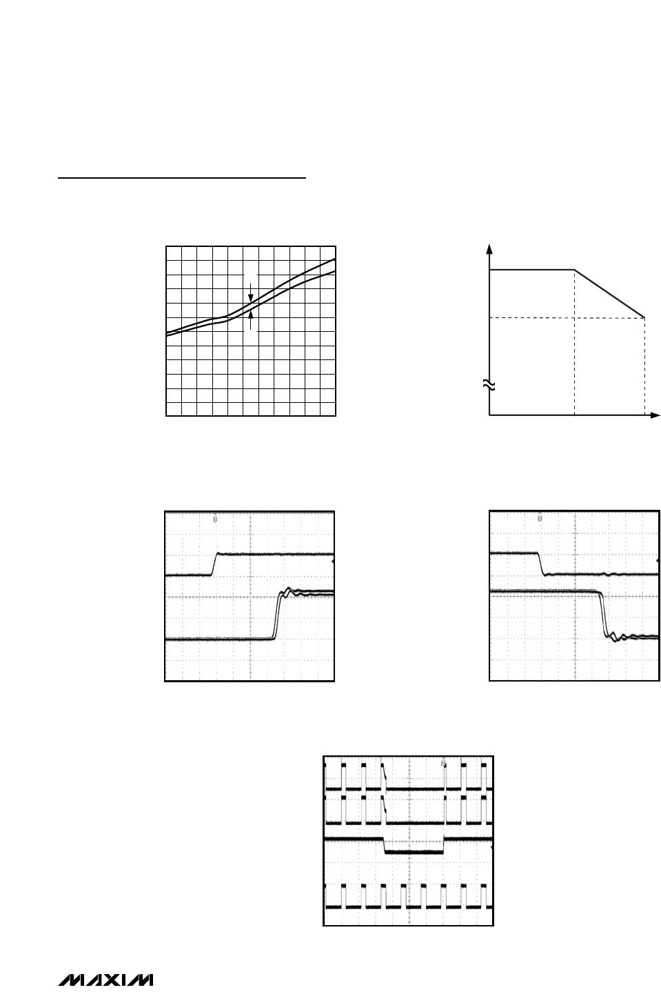
The maximum operating supply voltage (V
DD
) must be
reduced linearly from 12.6V to 10.5V when the maxi-
mum voltage (V
HS_MAX
) increases from 125V to 175V.
See the Typical Operating Characteristics.
Undervoltage Lockout
Both the high- and low-side drivers feature undervolt-
age lockout (UVLO). The low-side driver’s UVLO
LOW
threshold is referenced to GND and pulls both driver
outputs low when V
DD
falls below 6.8V. The high-side
driver has its own UVLO threshold (UVLO
HIGH
), refer-
enced to HS, and pulls DH low when BST falls below
6.4V with respect to HS.
During turn-on, once V
DD
rises above its UVLO thresh-
old, DL starts switching and follows the IN_L logic input.
At this time, the bootstrap capacitor is not charged and
the BST-to-HS voltage is below UVLO
BST
. For synchro-
nous buck and half-bridge converter topologies, the
bootstrap capacitor can charge up in one cycle and nor-
mal operation begins in a few microseconds after the
BST-to-HS voltage exceeds UVLO
BST
. In the two-switch
forward topology, the BST capacitor takes some time (a
few hundred microseconds) to charge and increase its
voltage above UVLO
BST
.
The typical hysteresis for both UVLO thresholds is 0.5V.
The bootstrap capacitor value should be selected care-
fully to avoid unintentional oscillations during turn-on
and turn-off at the DH output. Choose the capacitor
value about 20 times higher than the total gate capaci-
tance of the MOSFET. Use a low-ESR-type X7R dielec-
tric ceramic capacitor at BST (typically a 0.1µF ceramic
capacitor is adequate) and a parallel combination of
1µF and 0.1µF ceramic capacitors from V
DD
to GND.
The high-side MOSFET’s continuous on-time is limited
due to the charge loss from the high-side driver’s qui-
escent current. The maximum on-time is dependent on
the size of C
BST
, I
BST
(40µA max), and UVLO
BST
.
Output Driver
The MAX15012/MAX15013 have low 2.5Ω R
DS_ON
p-
channel and n-channel devices (totem pole) in the out-
put stage. This allows for a fast turn-on and turn-off of the
high gate-charge switching MOSFETs. The peak source
and sink current is typically 2A. Propagation delays from
the logic inputs to the driver outputs are matched to
within 8ns. The internal p- and n-channel MOSFETs have
a 1ns break-before-make logic to avoid any cross con-
duction between them. This internal break-before-make
logic eliminates shoot-through currents reducing the
operating supply current as well as the spikes at V
DD
.
See the Minimum Input Pulse Width section to under-
stand the effects of propagation delays on DH and DL.
The DL voltage is approximately equal to V
DD
, the DH-
to-HS voltage is approximately equal to V
DD
minus a
diode drop, when they are in a high state and to zero
when in a low state. The driver R
DS_ON
is lower at higher
V
DD
. Lower R
DS_ON
means higher source and sink cur-
rents and faster switching speeds.
Internal Bootstrap Diode
An internal diode connects from V
DD
to BST and is used
in conjunction with a bootstrap capacitor externally con-
nected between BST and HS. The diode charges the
capacitor from V
DD
when the DL low-side switch is on
and isolates V
DD
when HS is pulled high as the high-
side driver turns on (see the Typical Operating Circuit).
The internal bootstrap diode has a typical forward volt-
age drop of 0.9V and has a 10ns typical turn-off/turn-on
time. For lower voltage drops from V
DD
to BST, connect
an external Schottky diode between V
DD
and BST.
Driver Logic Inputs (IN_H, IN_L)
The MAX15012A/B/C/D are CMOS (V
DD
/2) logic-input
drivers while the MAX15013A/B/C/D have TTL-compati-
ble logic inputs. The logic-input signals are independent
of V
DD
. For example, the IC can be powered by a 10V
supply while the logic inputs are provided from a 12V
CMOS logic. Also, the logic inputs are protected against
voltage spikes up to 14V, regardless of the V
DD
voltage.
The TTL and CMOS logic inputs have 250mV and 1.6V
hysteresis, respectively, to avoid double pulsing during
transition. The logic inputs are high-impedance pins and
should not be left floating. The low 2.5pF input capaci-
tance reduces loading and increases switching speed.
The noninverting inputs are pulled down to GND and the
inverting inputs are pulled up to V
DD
internally using a
1MΩ resistor. The PWM output from the controller must
assume a proper state while powering up the device.
With the logic inputs floating, the DH and DL outputs pull
low as V
DD
rises up above the UVLO threshold.