Si824x
16 Preliminary Rev. 0.3
3.2. Typical Performance Characteristics (4.0 Amp)
The typical performance characteristics depicted in Figures 20 through 31 are for information purposes only. Refer
to Table 1 on page 5 for actual specification limits.
Figure 20. Rise/Fall Time vs. Supply Voltage
Figure 21. Propagation Delay vs. Supply
Voltage
Figure 22. Supply Current vs. Supply Voltage
Figure 23. Supply Current vs. Supply Voltage
Figure 24. Supply Current vs. Temperature
Figure 25. Rise/Fall Time vs. Load
0
2
4
6
8
10
9 1215182124
Rise/Fall Time (ns)
VDDA Supply (V)
VDD=12V, 25°C
C
L
= 100 pF
Tfall
Trise
10
15
20
25
30
9 1215182124
Propagation Delay (ns)
VDDA Supply (V)
H-L
L-H
VDD=12V, 25°C
C
L
= 100 pF
0
2
4
6
8
10
12
14
9 141924
VDDA Supply Current (mA)
VDDA Supply Voltage (V)
Duty Cycle = 50%
C
L
= 0 pF
1 Channel Switching
1MHz
500kHz
100kHz
50 kHz
0
2
4
6
8
10
12
14
9141924
VDDA Supply Current (mA)
VDDA Supply Voltage (V)
Duty Cycle = 50%
C
L
= 100 pF
1 Channel Switching
1MHz
500kHz
100kHz
50 kHz
0
2
4
6
8
10
-50 0 50 100
Supply Current (mA)
Temperature (°C)
VDDA = 15V,
f = 250kHz, C
L
= 0 pF
Duty Cycle = 50%
2 Channels Switching
0
5
10
15
20
25
30
35
40
012345678910
Rise/Fall Time (ns)
Load (nF)
VDD=12V, 25°C
Tfall
Trise
Si824x
Preliminary Rev. 0.3 17
Figure 26. Propagation Delay vs. Load
Figure 27. Propagation Delay vs. Temperature
Figure 28. Output Sink Current vs. Supply
Voltage
Figure 29. Output Source Current vs. Supply
Voltage
Figure 30. Output Sink Current vs. Temperature
Figure 31. Output Source Current vs.
Temperature
10
15
20
25
30
35
40
45
50
012345678910
Propagation Delay (ns)
Load (nF)
VDD=12V, 25°C
H-L
L-H
10
15
20
25
30
-40 -20 0 20 40 60 80 100 120
Propagation Delay (ns)
Temperature (°C)
VDD=12V, Load = 200pF
H-L
L-H
4
5
6
7
8
9
10 12 14 16 18 20 22 24
Sink Current (A)
Supply Voltage (V)
VDD=12V, Vout=5V
2
2.25
2.5
2.75
3
3.25
3.5
3.75
4
10 15 20 25
Source Current (A)
Supply Voltage (V)
VDD=12V, Vout=VDD-5V
4
4.25
4.5
4.75
5
5.25
5.5
5.75
6
6.25
6.5
6.75
7
-40 -10 20 50 80 110
Sink Current (A)
Temperature (°C)
VDD=12V, Vout=5V
2
2.25
2.5
2.75
3
3.25
3.5
-40 -10 20 50 80 110
Source Current (A)
Temperature (°C)
VDD=12V, Vout=VDD-5V
Si824x
18 Preliminary Rev. 0.3
3.3. Family Overview and Logic Operation During Startup
The Si824x family of isolated drivers consists of high-side, low-side, and dual driver configurations.
3.3.1. Products
Table 9 shows the configuration and functional overview for each product in this family.
3.3.2. Device Behavior
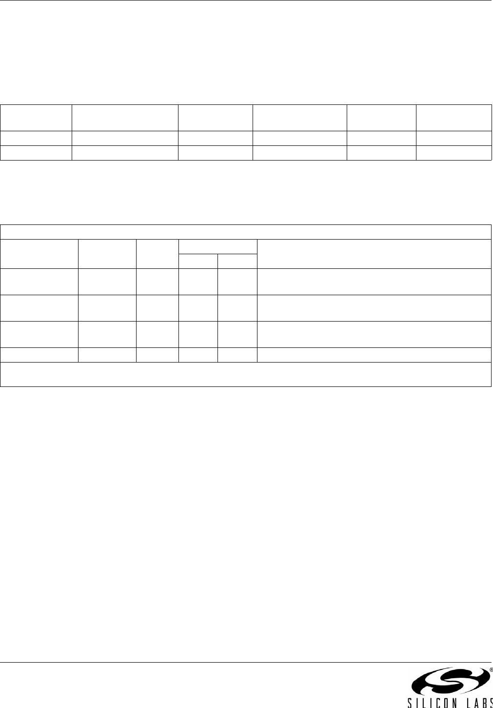
Table 10 contains truth tables for the Si8241/4 families.
Table 9. Si824x Family Overview
Part Number Configuration UVLO Voltage Programmable
Dead Time
Inputs Peak Output
Current (A)
Si8241 High-Side/Low-Side 8 V/10 V PWM 0.5
Si8244 High-Side/Low-Side 8 V/10 V PWM 4.0
Table 10. Si824x Family Truth Table*
Si8241/4 (PWM Input High-Side/Low-Side) Truth Table
PWM Input VDDI State Disable
Output
Notes
VOA VOB
H Powered L H L
Output transition occurs after internal dead time
expires.
L Powered L L H
Output transition occurs after internal dead time
expires.
X Unpowered X L L
Output returns to input state within 7 µs of VDDI
power restoration.
X Powered H L L Device is disabled.
*Note: This truth table assumes VDDA and VDDB are powered. If VDDA and VDDB are below UVLO, see
"3.7.2.Undervoltage Lockout" on page 21 for more information.

SI8244CB-D-IS1

Mfr. #:
Manufacturer:
Silicon Labs
Description:
Gate Drivers 2.5kV 4A Class D Audio Driver, 10V UVLO PWM input
Lifecycle:
New from this manufacturer.
Delivery:
DHL FedEx Ups TNT EMS
Payment:
T/T Paypal Visa MoneyGram Western Union