Si824x
22 Preliminary Rev. 0.3
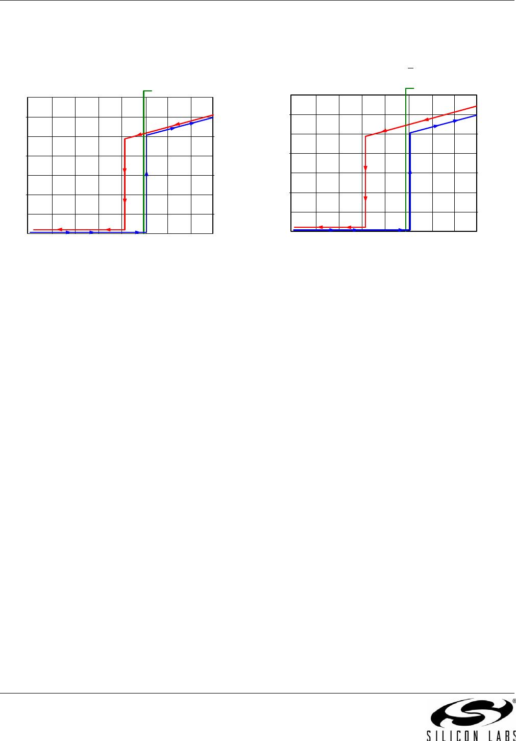
3.7.3. Undervoltage Lockout (UVLO)
The UVLO circuit unconditionally drives VO low when VDD is below the lockout threshold. Referring to Figures 35
and 36, upon power up, the Si824x is maintained in UVLO until VDD rises above VDD
UV+
. During power down, the
Si824x enters UVLO when VDD falls below the UVLO threshold plus hysteresis (i.e., VDD <
VDD
UV+
– VDD
HYS
).
Figure 35. Si824x UVLO Response (8 V)
Figure 36. Si824x UVLO Response (10 V)
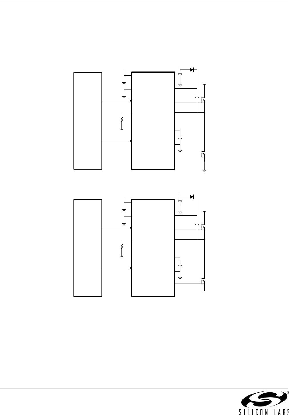
3.7.4. Control Inputs
PWM inputs are high-true, TTL level-compatible logic inputs. VOA is high and VOB is low when the PWM input is
high, and VOA is low and VOB is high when the PWM input is low.
3.7.5. Disable Input
When brought high, the DISABLE input unconditionally drives VOA and VOB low regardless of the states of input.
Device operation terminates within tSD after DISABLE = V
IH
and resumes within tRESTART after DISABLE = V
IL
.
The DISABLE input has no effect if VDDI is below its UVLO level (i.e. VOA, VOB remain low). The DISABLE input
is typically connected to external protection circuitry to unconditionally halt driver operation in the event of a fault.
6.0
10.5
V
DDUV+
(Typ)
Output Voltage (V
O
)
6.5 7.0 7.5 8.0 8.5 9.0 9.5 10.0
Supply Voltage (V
DD
- V
SS
) (V)
8.5
10.5
V
DDUV+
(Typ)
Output Voltage (V
O
)
9.0 9.5 10.0 10.5 11.0 11.5 12.0 12.5
Supply Voltage (V
DD
- V
SS
) (V)
Si824x
Preliminary Rev. 0.3 23
3.8. Programmable Dead Time and Overlap Protection
All high-side/low-side drivers (Si8241/4) include programmable overlap protection to prevent outputs VOA and
VOB from being high at the same time. These devices also include programmable dead time, which adds a user-
programmable delay between transitions of VOA and VOB. When enabled, dead time is present on all transitions,
even after overlap recovery. The amount of dead time delay (DT) is programmed by a single resistor (RDT)
connected from the DT input to ground per Equation 5. Minimum dead time (approximately 400 ps) can be
achieved by connecting the DT pin to VDDI. Note that dead time accuracy is limited by the resistor’s (R
DT
)
tolerance and temperature coefficient. See Figures 37 and 38 for additional information about dead time operation.
Equation 5.
Figure 37. Dead Time vs.Resistance (R
DT
)
Figure 38. Dead Time vs.Temperature
DT 10 RDT
where:
DT dead time (ns)
and
RDT dead time programming resistor (k=
=
0
100
200
300
400
500
600
700
800
900
1000
0 20 40 60 80 100
Dead-time (ns)
Dead-time Resistance (k::)
0
10
20
30
40
50
60
70
80
90
100
-40 -20 0 20 40 60 80 100 120
Dead-time (ns)
Temperature (°C)
R
DT
= 4k
R
DT
= 10k
R
DT
= 3k
R
DT
= 5k
R
DT
= 6k
R
DT
= 2k
R
DT
= 1k
R
DT
=0
Si824x
24 Preliminary Rev. 0.3
4. Applications
The following examples illustrate typical circuit configurations using the Si824x.
4.1. Class D Digital Audio Driver
Figures 39 and 40 show the Si8241/4 controlled by a single PWM signal. Supply can be unipolar (0 to 1500 V) or
bipolar (± 750 V).
Figure 39. Si824x in Half-Bridge Audio Application
Figure 40. Si824x in Half-Bridge Audio Application
D1 and CB form a conventional bootstrap circuit that allows VOA to operate as a high-side driver for Q1, which has
a maximum drain voltage of 1500 V. VOB is connected as a conventional low-side driver. Note that the input side of
the Si824x requires VDD in the range of 4.5 to 5.5 V, while the VDDA and VDDB output side supplies must be
between 6.5 and 24 V with respect to their respective grounds. The boot-strap start up time will depend on the CB
cap chosen. VDD2 is usually the same as VDDB. Also note that the bypass capacitors on the Si824x should be
located as close to the chip as possible. Moreover, it is recommended that 0.1 and 10 µF bypass capacitors be
used to reduce high frequency noise and maximize performance. The D1 diode should be a fast-recovery diode; it
should be able to withstand the maximum high voltage (e.g. 1500 V) and be low-loss. See “AN486: High-Side
Bootstrap Design Using Si823x ISODrivers in Power Delivery Systems” for more details in selecting the bootstrap
cap (CB) and diode (D1).
Si8241/4
CB
GNDI
VDDI
PWM
VDDA
VOA
GNDA
VOB
VDDI
VDDB
GNDB
DISABLE
DT
RDT
CONTROLLER
C1
1uF
PWMOUT
I/O
Q1
Q2
D1
VDDB
C3
10uF
VDD2
C2
1 µF
1500 V max
Si8241/4
CB
GNDI
VDDI
PWM
VDDA
VOA
GNDA
VOB
VDDI
VDDB
GNDB
DISABLE
DT
RDT
CONTROLLER
C1
1uF
PWMOUT
I/O
Q1
Q2
D1
VDDB
C3
10uF
VDD2
C2
1 µF
+750 V max
-750 V max

SI8244CB-D-IS1

Mfr. #:
Manufacturer:
Silicon Labs
Description:
Gate Drivers 2.5kV 4A Class D Audio Driver, 10V UVLO PWM input
Lifecycle:
New from this manufacturer.
Delivery:
DHL FedEx Ups TNT EMS
Payment:
T/T Paypal Visa MoneyGram Western Union