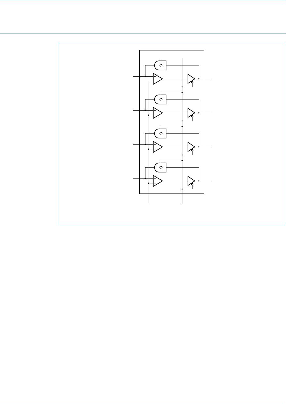
1. General description
The GTL2014 is a 4-bit translating transceiver designed for 3.3 V LVTTL system interface
with a GTL/GTL/GTL+ bus, where GTL/GTL/GTL+ refers to the reference voltage of the
GTL bus and the input/output voltage thresholds associated with it.
The direction pin allows the part to function as either a GTL to LVTTL sampling receiver or
as a LVTTL to GTL interface.
The GTL2014 LVTTL inputs (only) are tolerant up to 5.5 V allowing direct access to TTL or
5 V CMOS inputs. The LVTTL outputs are not 5.5 V tolerant.
The GTL2014 GTL inputs and outputs operate up to 3.6 V, allowing the device to be used
in higher voltage open-drain output applications.
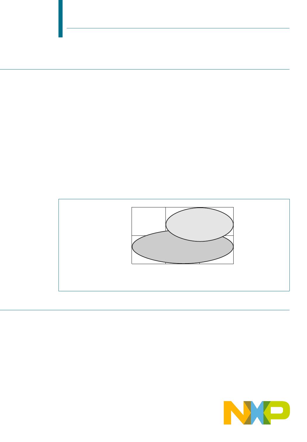
GTL2014 is pin-to-pin backward compatible to the GTL2005 (labels for A port and B port
are interchanged). GTL2014’s V
ref
tracks down to 0.5 V for low voltage CPU, propagation
delays are slightly longer, while GTL2005’s V
ref
linearity degrades below 0.8 V and has
shorter propagation delay.
2. Features and benefits
Operates as a 4-bit GTL/GTL/GTL+ sampling receiver or as a LVTTL to
GTL/GTL/GTL+ driver
3.0 V to 3.6 V operation with 5 V tolerant LVTTL input
GTL input and output 3.6 V tolerant
V
ref
adjustable from 0.5 V to V
CC
/2
Partial power-down permitted
ESD protection exceeds 2000 V HBM per JESD22-A114 and 1000 V CDM per
JESD22-CC101
GTL2014
4-bit LVTTL to GTL transceiver
Rev. 3 — 14 June 2012 Product data sheet
Fig 1. GTL2005/GTL2014 positioning
002aab378
GTL
GTL
GTL+
fast t
PD
slow t
PD
GTL2014
GTL2005
GTL2014 All information provided in this document is subject to legal disclaimers. © NXP B.V. 2012. All rights reserved.
Product data sheet Rev. 3 — 14 June 2012 2 of 19
NXP Semiconductors
GTL2014
4-bit LVTTL to GTL transceiver
Latch-up protection exceeds 500 mA per JESD78
Package offered: TSSOP14
3. Quick reference data
4. Ordering information
Standard packing quantities and other packaging data are available at
www.nxp.com/packages/
.
4.1 Ordering options
Table 1. Quick reference data
T
amb
=25
°
C
Symbol Parameter Conditions Min Typ Max Unit
t
PLH
LOW to HIGH propagation delay An-to-Bn; C
L
=50pF; V
CC
= 3.3 V - 2.8 - ns
t
PHL
HIGH to LOW propagation delay An-to-Bn; C
L
=50pF; V
CC
= 3.3 V - 3.4 - ns
t
PLH
LOW to HIGH propagation delay Bn-to-An; C
L
=50pF; V
CC
= 3.3 V - 5.2 - ns
t
PHL
HIGH to LOW propagation delay Bn-to-An; C
L
=50pF; V
CC
= 3.3 V - 4.9 - ns
C
i
input capacitance control inputs; V
I
= 3.0 V or 0 V - 2 2.5 pF
C
io
input/output capacitance A port; V
O
= 3.0 V or 0 V - 4.6 6 pF
B port; V
O
=V
TT
or 0 V - 3.4 4.3 pF
Table 2. Ordering information
Type number Package
Name Description Version
GTL2014PW TSSOP14 plastic thin shrink small outline package; 14 leads; body width 4.4 mm SOT402-1
Table 3. Ordering options
Type number Topside mark Temperature range
GTL2014PW GTL2014 T
amb
= 40 °Cto +85°C
GTL2014 All information provided in this document is subject to legal disclaimers. © NXP B.V. 2012. All rights reserved.
Product data sheet Rev. 3 — 14 June 2012 3 of 19
NXP Semiconductors
GTL2014
4-bit LVTTL to GTL transceiver
5. Functional diagram
Fig 2. Logic diagram for GTL2014
002aab139
GTL2014
A0
A1
A2
A3
B0
B1
B2
B3
VREF DIR

GTL2014PW,118

Mfr. #:
Manufacturer:
NXP Semiconductors
Description:
Bus Transceivers 4-BIT BI-DIREC NON-LATCH TRAN
Lifecycle:
New from this manufacturer.
Delivery:
DHL FedEx Ups TNT EMS
Payment:
T/T Paypal Visa MoneyGram Western Union

Products related to this Datasheet