NOVEMBER 1997 - REVISED JANUARY 2007
Specifications are subject to change without notice.
Customers should verify actual device performance in their specific applications.
Electrical Characteristics, T
A
= 25 °C (Unless Otherwise Noted)
TISP4xxxH3BJ Overvoltage Protector Series
Parameter Test Conditions Min. Typ. Max. Unit
I
DRM
Repetitive peak off-
state current
V
D
= V
DRM
T
A
= 25 °C
T
A
= 85 °C
±5
±10
µA
V
(BO)
Breakover voltage dv/dt = ±750 V/ms, R
SOURCE
= 300
‘4070
‘4080
‘4095
‘4115
‘4125
‘4145
‘4165
‘4180
‘4200
‘4220
‘4240
‘4250
‘4265
‘4290
‘4300
‘4350
‘4395
‘4400
±70
±80
±95
±115
±125
±145
±165
±180
±200
±220
±240
±250
±265
±290
±300
±350
±395
±400
V
V
(BO)
Impulse breakover
voltage
dv/dt
±1000 V/µs, Linear voltage ramp,
Maximum ramp value = ±500 V
di/dt = ±20 A/µs, Linear current ramp,
Maximum ramp value = ±10 A
‘4070
‘4080
‘4095
‘4115
‘4125
‘4145
‘4165
‘4180
‘4200
‘4220
‘4240
‘4250
‘4265
‘4290
‘4300
‘4350
‘4395
‘4400
±78
±88
±103
±124
±134
±154
±174
±189
±210
±230
±250
±261
±276
±301
±311
±362
±408
±413
V
I
(BO)
Breakover current dv/dt = ±750 V/ms, R
SOURCE
= 300 ±0.15 ±0.6 A
V
T
On-state voltage I
T
= ±5A, t
W
= 100 µs ±3V
I
H
Holding current I
T
= ±5A, di/dt=-/+30mA/ms ±0.15 ±0.6 A
dv/dt
Critical rate of rise of
off-state voltage
Linear voltage ramp, Maximum ramp value < 0.85V
DRM
±5kV/µs
I
D
Off-state current V
D
= ±50 V T
A
= 85 °C ±10 µA
NOVEMBER 1997 - REVISED JANUARY 2007
Specifications are subject to change without notice.
Customers should verify actual device performance in their specific applications.
Electrical Characteristics, T
A
= 25 °C (Unless Otherwise Noted) (continued)
TISP4xxxH3BJ Overvoltage Protector Series
C
off
Off-state capacitance
f = 100 kHz, V
d
=1V rms, V
D
=0,
f = 100 kHz, V
d
=1V rms, V
D
=-1V
f = 100 kHz, V
d
=1V rms, V
D
=-2V
f = 100 kHz, V
d
=1V rms, V
D
=-50V
f = 100 kHz, V
d
=1V rms, V
D
= -100 V
(see Note 6)
‘4070 thru ‘4115
‘4125 thru ‘4220
‘4240 thru ‘4400
‘4070 thru ‘4115
‘4125 thru ‘4220
‘4240 thru ‘4400
‘4070 thru ‘4115
‘4125 thru ‘4220
‘4240 thru ‘4400
‘4070 thru ‘4115
‘4125 thru ‘4220
‘4240 thru ‘4400
‘4125 thru ‘4220
‘4240 thru ‘4400
145
80
70
130
71
60
120
65
55
62
30
24
28
22
170
90
84
150
79
67
140
74
62
73
35
28
33
26
pF
NOTE 6: To avoid possible voltage clipping, the ‘4125 is tested with V
D
=-98V.
Parameter Test Conditions Min. Typ. Max. Unit
Thermal Characteristics
Parameter Test Conditions Min. Typ. Max. Unit
R
θJA
Junction to free air thermal resistance
EIA/JESD51-3 PCB, I
T
= I
TSM(1000)
,
T
A
= 25 °C, (see Note 7)
113
°C/W
265 mm x 210 mm populated line card,
4-layer PCB, I
T
= I
TSM(1000)
, T
A
= 25 °C
50
NOTE 7: EIA/JESD51-2 environment and PCB has standard footprint dimensions connected with 5 A rated printed wiring track widths.
NOVEMBER 1997 - REVISED JANUARY 2007
Specifications are subject to change without notice.
Customers should verify actual device performance in their specific applications.
Parameter Measurement Information
TISP4xxxH3BJ Overvoltage Protector Series
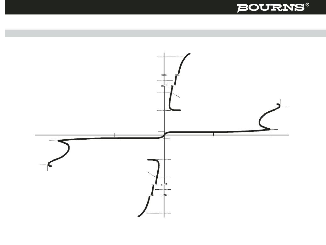
Figure 1. Voltage-current Characteristic for T and R Terminals
All Measurements are Referenced to the R Terminal
-v
V
DRM
I
DRM
V
D
I
H
I
T
V
T
I
TSM
I
TSP
V
(BO)
I
(BO)
I
D
Quadrant I
Switching
Characteristic
+v
+i
V
(BO)
I
(BO)
V
D
I
D
I
H
I
T
V
T
I
TSM
I
TSP
-i
Quadrant III
Switching
Characteristic
PMXXAAB
V
DRM
I
DRM

TISP4395H3BJR-S

Mfr. #:
Manufacturer:
Bourns
Description:
Thyristor Surge Protection Devices (TSPD) 320V
Lifecycle:
New from this manufacturer.
Delivery:
DHL FedEx Ups TNT EMS
Payment:
T/T Paypal Visa MoneyGram Western Union