74LVC_LVCH1T45 All information provided in this document is subject to legal disclaimers. © NXP B.V. 2012. All rights reserved.
Product data sheet Rev. 6 — 6 August 2012 11 of 33
NXP Semiconductors
74LVC1T45; 74LVCH1T45
Dual supply translating transceiver; 3-state
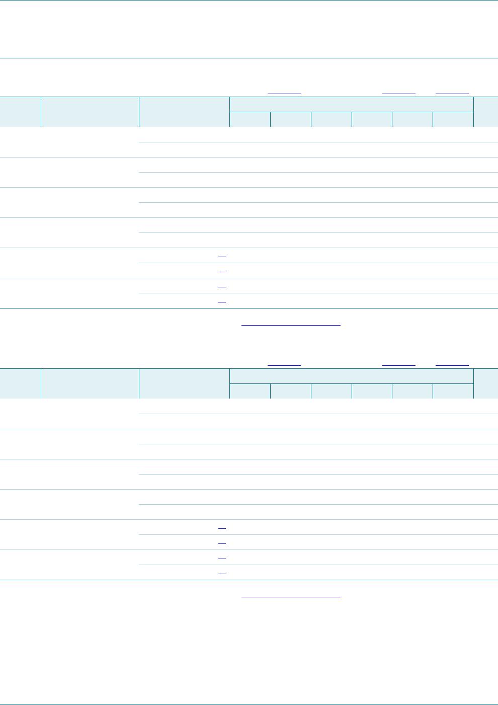
t
PZH
OFF-statetoHIGH
propagation delay
DIR to A
[1]
- 35.2 - 33.7 - 25.2 - 23.9 - 21.8 ns
DIR to B
[1]
- 29.6 - 28.2 - 19.8 - 17.7 - 17.3 ns
t
PZL
OFF-state to LOW
propagation delay
DIR to A
[1]
- 39.4 - 36.2 - 24.4 - 22.9 - 20.4 ns
DIR to B
[1]
- 34.4 - 31.4 - 25.6 - 24.2 - 24.1 ns
V
CC(A)
= 2.3 V to 2.7 V
t
PLH
LOW to HIGH
propagation delay
A to B 2.3 17.9 2.3 16.0 1.5 8.5 1.3 6.2 1.1 4.8 ns
B to A 2.0 13.5 2.2 9.3 1.5 8.5 1.4 8.0 1.0 7.5 ns
t
PHL
HIGH to LOW
propagation delay
A to B 2.3 15.8 2.1 12.9 1.4 7.5 1.3 5.4 0.9 4.6 ns
B to A 1.8 11.8 1.9 8.5 1.4 7.5 1.3 7.0 0.9 6.2 ns
t
PHZ
HIGH to OFF-state
propagation delay
DIR to A 2.1 8.1 2.1 8.1 2.1 8.1 2.1 8.1 2.1 8.1 ns
DIR to B 3.0 22.5 3.0 21.4 2.5 11.0 2.8 9.3 2.3 6.9 ns
t
PLZ
LOW to OFF-state
propagation delay
DIR to A 1.7 5.8 1.7 5.8 1.7 5.8 1.7 5.8 1.7 5.8 ns
DIR to B 2.3 14.6 2.5 13.2 2.0 9.0 2.5 8.4 1.8 5.3 ns
t
PZH
OFF-statetoHIGH
propagation delay
DIR to A
[1]
- 28.1 - 22.5 - 17.5 - 16.4 - 12.8 ns
DIR to B
[1]
- 23.7 - 21.8 - 14.3 - 12.0 - 10.6 ns
t
PZL
OFF-state to LOW
propagation delay
DIR to A
[1]
- 34.3 - 29.9 - 18.5 - 16.3 - 13.1 ns
DIR to B
[1]
- 23.9 - 21.0 - 15.6 - 13.5 - 12.7 ns
V
CC(A)
= 3.0V to 3.6V
t
PLH
LOW to HIGH
propagation delay
A to B 2.3 17.1 2.1 15.5 1.4 8.0 0.8 5.6 0.7 4.4 ns
B to A 1.7 11.8 1.7 7.2 1.3 6.2 0.7 5.6 0.6 5.4 ns
t
PHL
HIGH to LOW
propagation delay
A to B 2.2 15.6 2.0 12.6 1.3 7.0 0.8 5.0 0.7 4.0 ns
B to A 1.7 10.9 1.8 7.1 1.3 5.4 0.8 5.0 0.7 4.5 ns
t
PHZ
HIGH to OFF-state
propagation delay
DIR to A 2.3 7.3 2.3 7.3 2.3 7.3 2.3 7.3 2.7 7.3 ns
DIR to B 2.9 18.0 2.9 16.5 2.3 10.1 2.7 8.6 2.2 6.3 ns
t
PLZ
LOW to OFF-state
propagation delay
DIR to A 2.0 5.6 2.0 5.6 2.0 5.6 2.0 5.6 2.0 5.6 ns
DIR to B 2.3 13.6 2.4 12.5 1.9 7.8 2.3 7.1 1.7 4.9 ns
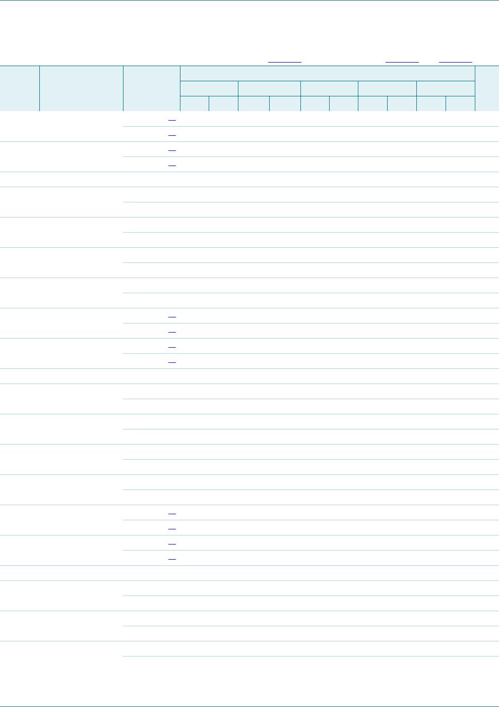
t
PZH
OFF-statetoHIGH
propagation delay
DIR to A
[1]
- 25.4 - 19.7 - 14.0 - 12.7 - 10.3 ns
DIR to B
[1]
- 22.7 - 21.1 - 13.6 - 11.2 - 10.0 ns
t
PZL
OFF-state to LOW
propagation delay
DIR to A
[1]
- 28.9 - 23.6 - 15.5 - 13.6 - 10.8 ns
DIR to B
[1]
- 22.9 - 19.9 - 14.3 - 12.3 - 11.3 ns
V
CC(A)
= 4.5V to 5.5V
t
PLH
LOW to HIGH
propagation delay
A to B 2.2 16.6 1.9 15.1 1.0 7.5 0.7 5.4 0.5 3.9 ns
B to A 1.6 10.5 1.4 6.8 1.0 4.8 0.7 4.4 0.5 3.9 ns
t
PHL
HIGH to LOW
propagation delay
A to B 2.3 15.3 1.8 12.2 1.0 6.2 0.7 4.5 0.5 3.5 ns
B to A 1.7 10.8 1.7 7.0 0.9 4.6 0.7 4.0 0.5 3.5 ns
t
PHZ
HIGH to OFF-state
propagation delay
DIR to A 1.7 5.4 1.7 5.4 1.7 5.4 1.7 5.4 1.7 5.4 ns
DIR to B 2.9 17.3 2.9 16.1 2.3 9.7 2.7 8.0 2.5 5.7 ns
Table 12. Dynamic characteristics for temperature range 40 C to +85 C
…continued
Voltages are referenced to GND (ground = 0 V); for test circuit see Figure 8; for wave forms see Figure 6 and Figure 7
Symbol Parameter Conditions V
CC(B)
Unit
1.5 V 0.1 V 1.8 V 0.15 V 2.5 V 0.2 V 3.3 V 0.3 V 5.0 V 0.5 V
Min Max Min Max Min Max Min Max Min Max