74LVC_LVCH1T45 All information provided in this document is subject to legal disclaimers. © NXP B.V. 2012. All rights reserved.
Product data sheet Rev. 6 — 6 August 2012 21 of 33
NXP Semiconductors
74LVC1T45; 74LVCH1T45
Dual supply translating transceiver; 3-state
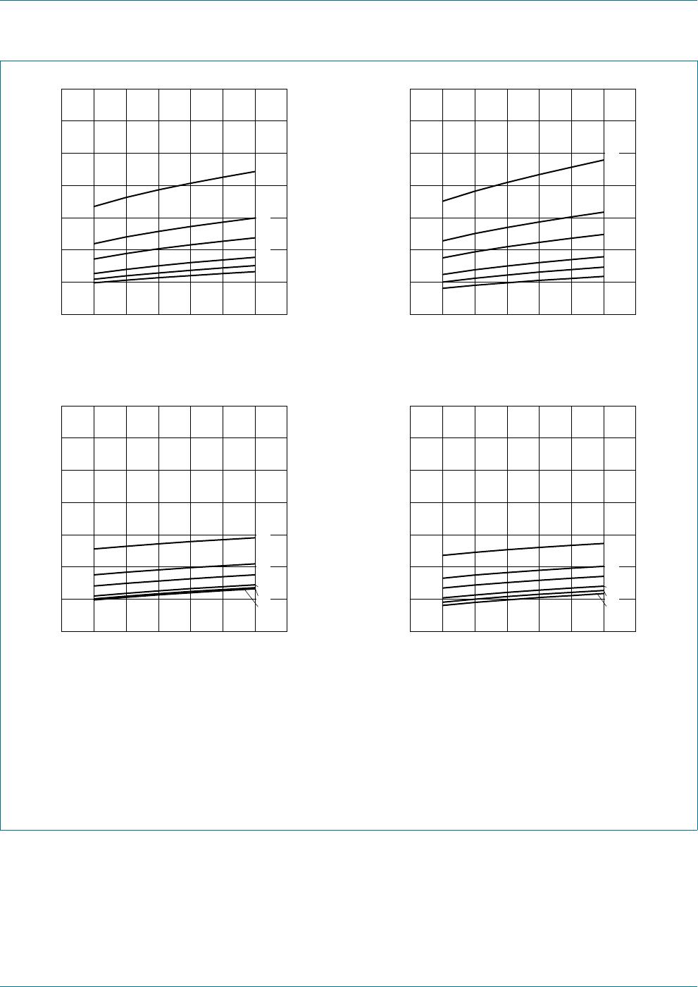
a. HIGH to LOW propagation delay (A to B) b. LOW to HIGH propagation delay (A to B)
c. HIGH to LOW propagation delay (B to A) d. LOW to HIGH propagation delay (B to A)
(1) V
CC(B)
= 1.2 V.
(2) V
CC(B)
= 1.5 V.
(3) V
CC(B)
= 1.8 V.
(4) V
CC(B)
= 2.5 V.
(5) V
CC(B)
= 3.3 V.
(6) V
CC(B)
= 5.0 V.
Fig 14. Typical propagation delay vs load capacitance; T
amb
= 25 C; V
CC(A)
=5V
C
L
(pF)
035
001aai927
14
t
PHL
(ns)
0
2
4
6
8
10
12
5 1015202530
(1)
(5)
(4)
(2)
(3)
(6)
C
L
(pF)
035
001aai928
14
t
PLH
(ns)
0
2
4
6
8
10
12
5 1015202530
(1)
(5)
(4)
(2)
(3)
(6)
C
L
(pF)
035
001aai929
14
t
PHL
(ns)
0
2
4
6
8
10
12
5 1015202530
(1)
(5)
(4)
(2)
(3)
(6)
C
L
(pF)
035
001aai930
14
t
PLH
(ns)
0
2
4
6
8
10
12
5 1015202530
(1)
(5)
(4)
(2)
(3)
(6)
74LVC_LVCH1T45 All information provided in this document is subject to legal disclaimers. © NXP B.V. 2012. All rights reserved.
Product data sheet Rev. 6 — 6 August 2012 22 of 33
NXP Semiconductors
74LVC1T45; 74LVCH1T45
Dual supply translating transceiver; 3-state
14. Application information
14.1 Unidirectional logic level-shifting application
The circuit given in Figure 15 is an example of the 74LVC1T45; 74LVCH1T45 being used
in a unidirectional logic level-shifting application.
Fig 15. Unidirectional logic level-shifting application
Table 16. Description unidirectional logic level-shifting application
Pin Name Function Description
1V
CC(A)
V
CC1
supply voltage of system-1 (1.2 V to 5.5 V)
2 GND GND device GND
3 A OUT output level depends on V
CC1
voltage
4 B IN input threshold value depends on V
CC2
voltage
5 DIR DIR the GND (LOW level) determines B port to A port direction
6V
CC(B)
V
CC2
supply voltage of system-2 (1.2 V to 5.5 V)
001aaj994
74LVC1T45
74LVCH1T45
V
CC1
V
CC2
V
CC1
1
2
3
V
CC(A)
GND
system-1 system-2
A
6
5
4
V
CC(B)
DIR
B
V
CC2
74LVC_LVCH1T45 All information provided in this document is subject to legal disclaimers. © NXP B.V. 2012. All rights reserved.
Product data sheet Rev. 6 — 6 August 2012 23 of 33
NXP Semiconductors
74LVC1T45; 74LVCH1T45
Dual supply translating transceiver; 3-state
14.2 Bidirectional logic level-shifting application
Figure 16 shows the 74LVC1T45; 74LVCH1T45 being used in a bidirectional logic
level-shifting application. Since the device does not have an output enable pin, the system
designer should take precautions to avoid bus contention between system-1 and
system-2 when changing directions.
Table 17 provides a sequence that illustrates data transmission from system-1 to
system-2 and then from system-2 to system-1.
[1] H = HIGH voltage level;
L = LOW voltage level;
Z = high-impedance OFF-state.
Pull-up or pull-down only needed for 74LVC1T45.
Fig 16. Bidirectional logic level-shifting application
Table 17. Description bidirectional logic level-shifting application
[1]
State DIR CTRL I/O-1 I/O-2 Description
1 H output input system-1 data to system-2
2 H Z Z system-2 is getting ready to send data to system-1.
I/O-1 and I/O-2 are disabled. The bus-line state
depends on bus hold.
3 L Z Z DIR bit is set LOW. I/O-1 and I/O-2 are still disabled.
The bus-line state depends on bus hold.
4 L input output system-2 data to system-1
001aaj995
74LVC1T45
74LVCH1T45
V
CC1
V
CC1
V
CC2
V
CC2
1
2
3
V
CC(A)
GND
system-1 system-2
A
6
5
4
V
CC(B)
DIR
B
I/O-1 I/O-2
PULL-UP/DOWN
DIR CTRL
PULL-UP/DOWN
74LVC1T45GW,125

Mfr. #:
Manufacturer:
Nexperia
Description:
Bus Transceivers Single-Bit Dual Sply 5.5V 250mW
Lifecycle:
New from this manufacturer.
Delivery:
DHL FedEx Ups TNT EMS
Payment:
T/T Paypal Visa MoneyGram Western Union