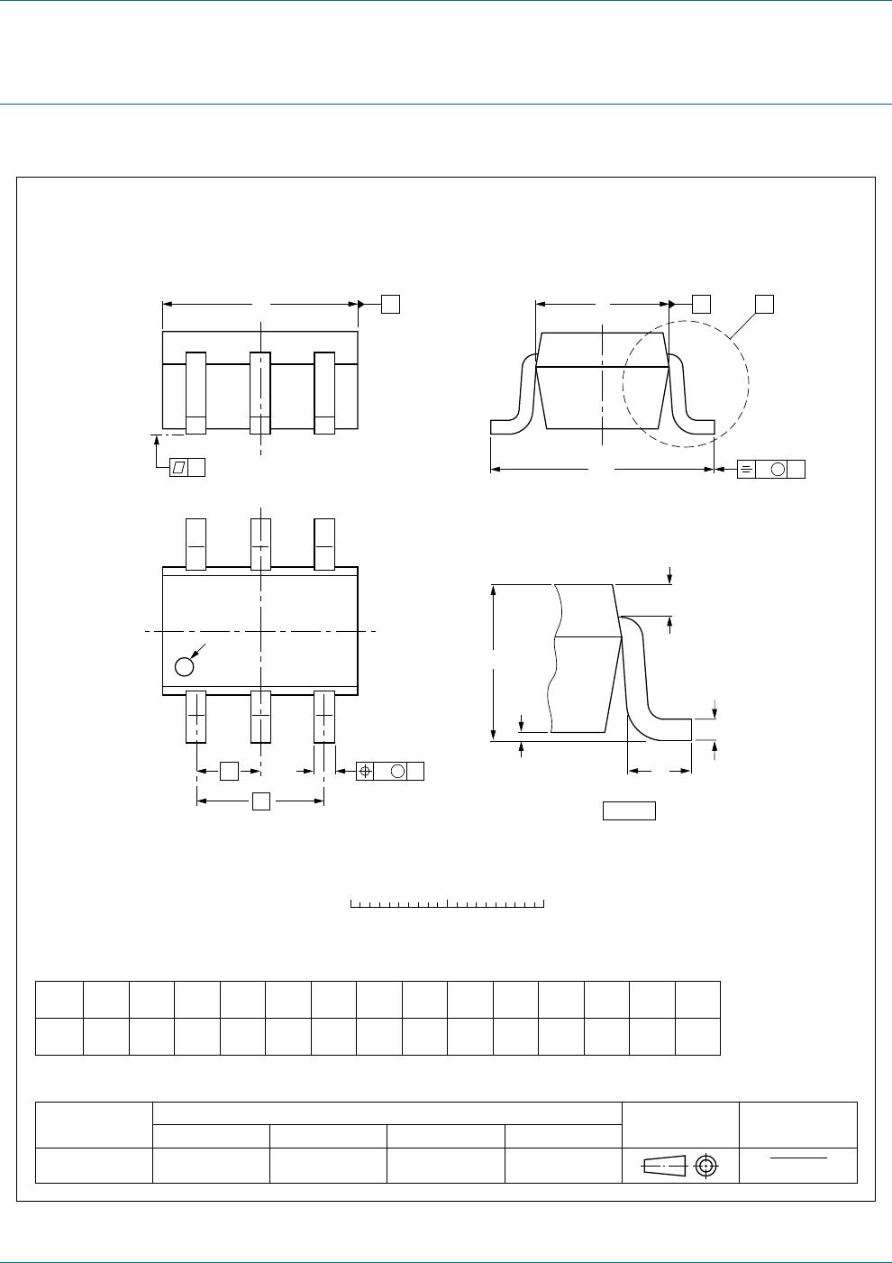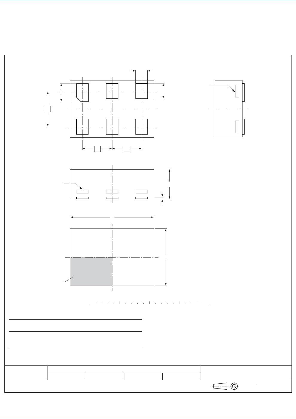
74LVC_LVCH1T45 All information provided in this document is subject to legal disclaimers. © NXP B.V. 2012. All rights reserved.
Product data sheet Rev. 6 — 6 August 2012 24 of 33
NXP Semiconductors
74LVC1T45; 74LVCH1T45
Dual supply translating transceiver; 3-state
14.3 Power-up considerations
The device is designed such that no special power-up sequence is required other than
GND being applied first.
14.4 Enable times
Calculate the enable times for the 74LVC1T45; 74LVCH1T45 using the following
formulas:
• t
PZH
(DIR to A) = t
PLZ
(DIR to B) + t
PLH
(B to A)
• t
PZL
(DIR to A) = t
PHZ
(DIR to B) + t
PHL
(B to A)
• t
PZH
(DIR to B) = t
PLZ
(DIR to A) + t
PLH
(A to B)
• t
PZL
(DIR to B) = t
PHZ
(DIR to A) + t
PHL
(A to B)
In a bidirectional application, these enable times provide the maximum delay from the
time the DIR bit is switched until an output is expected. For example, if the 74LVC1T45;
74LVCH1T45 initially is transmitting from A to B, then the DIR bit is switched, the B port of
the device must be disabled before presenting it with an input. After the B port has been
disabled, an input signal applied to it appears on the corresponding A port after the
specified propagation delay.
Table 18. Typical total supply current (I
CC(A)
+ I
CC(B)
)
V
CC(A)
V
CC(B)
Unit
0 V 1.8 V 2.5 V 3.3 V 5.0 V
0 V0 < 1< 1< 1< 1A
1.8 V < 1 < 2 < 2 < 2 2 A
2.5 V < 1 < 2 < 2 < 2 < 2 A
3.3 V < 1 < 2 < 2 < 2 < 2 A
5.0 V < 1 2 < 2 < 2 < 2 A