74LVC_LVCH1T45 All information provided in this document is subject to legal disclaimers. © NXP B.V. 2012. All rights reserved.
Product data sheet Rev. 6 — 6 August 2012 5 of 33
NXP Semiconductors
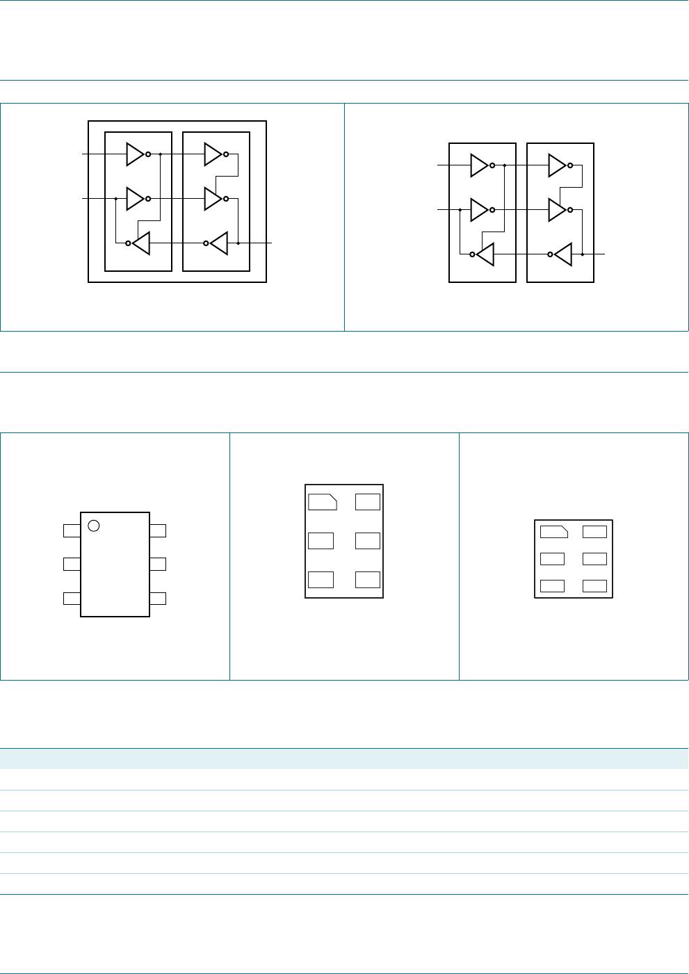
74LVC1T45; 74LVCH1T45
Dual supply translating transceiver; 3-state
[1] V
CCO
is the supply voltage associated with the output port.
[2] V
CCI
is the supply voltage associated with the input port.
10. Static characteristics
[1] V
CCO
is the supply voltage associated with the output port.
[2] V
CCI
is the supply voltage associated with the data input port.
[3] To guarantee the node switches, an external driver must source/sink at least I
BHLO
/I
BHHO
when the input is in the range V
IL
to V
IH
.
V
O
output voltage Active mode
[1]
0V
CCO
V
Suspend or 3-state mode 0 5.5 V
T
amb
ambient temperature 40 +125 C
t/V input transition rise and fall rate V
CCI
= 1.2 V
[2]
- 20 ns/V
V
CCI
= 1.4 V to 1.95 V - 20 ns/V
V
CCI
= 2.3 V to 2.7 V - 20 ns/V
V
CCI
= 3 V to 3.6 V - 10 ns/V
V
CCI
= 4.5 V to 5.5 V - 5 ns/V
Table 6. Recommended operating conditions …continued
Symbol Parameter Conditions Min Max Unit
Table 7. Typical static characteristics at T
amb
= 25 C
At recommended operating conditions; voltages are referenced to GND (ground = 0 V).
Symbol Parameter Conditions Min Typ Max Unit
V
OH
HIGH-level output voltage V
I
= V
IH
or V
IL
I
O
= 3 mA; V
CCO
=1.2V
[1]
-1.09-V
V
OL
LOW-level output voltage V
I
= V
IH
or V
IL
I
O
= 3 mA; V
CCO
=1.2V
[1]
-0.07-V
I
I
input leakage current DIR input; V
I
= 0 V to 5.5 V;
V
CCI
= 1.2 V to 5.5 V
[2]
-- 1 A
I
BHL
bus hold LOW current A or B port; V
I
=0.42V;V
CCI
=1.2V
[2]
-19-A
I
BHH
bus hold HIGH current A or B port; V
I
=0.78V;V
CCI
=1.2V
[2]
- 19 - A
I
BHLO
bus hold LOW overdrive
current
A or B port; V
CCI
= 1.2 V
[2][3]
-19-A
I
BHHO
bus hold HIGH overdrive
current
A or B port; V
CCI
= 1.2 V
[2][3]
- 19 - A
I
OZ
OFF-state output current A or B port; V
O
=0 Vor V
CCO
;
V
CCO
= 1.2 V to 5.5 V
[1]
-- 1 A
I
OFF
power-off leakage current A port; V
I
or V
O
= 0 V to 5.5 V;
V
CC(A)
=0V;V
CC(B)
= 1.2 V to 5.5 V
-- 1 A
B port; V
I
or V
O
= 0 V to 5.5 V;
V
CC(B)
=0V;V
CC(A)
= 1.2 V to 5.5 V
-- 1 A
C
I
input capacitance DIR input; V
I
= 0 V or 3.3 V;
V
CC(A)
=V
CC(B)
=3.3V
-2.2-pF
C
I/O
input/output capacitance A and B port; suspend mode;
V
O
=3.3Vor0V; V
CC(A)
=V
CC(B)
=3.3V
-6.0-pF