1
JULY 2013
CMOS SyncFIFO™
64 x 8, 256 x 8,
512 x 8, 1,024 x 8,
2,048 x 8 and 4,096 x 8
IDT72420
IDT72200
IDT72210
IDT72220
IDT72230
IDT72240
IDT, IDT logo are registered trademarks of Integrated Device Technology, Inc. The SyncFIFO is a trademark of Integrated Device Technology, Inc.
COMMERCIAL TEMPERATURE RANGE
©2013 Integrated Device Technology, Inc. All rights reserved. Product specifications subject to change without notice. DSC-2680/6
DESCRIPTION:
The IDT72420/72200/72210/72220/72230/72240 SyncFIFO™ are very
high-speed, low-power First-In, First-Out (FIFO) memories with clocked read
and write controls. These devices have a 64, 256, 512, 1,024, 2,048, and 4,096
x 8-bit memory array, respectively. These FIFOs are applicable for a wide
variety of data buffering needs, such as graphics, Local Area Networks (LANs),
and interprocessor communication.
These FIFOs have 8-bit input and output ports. The input port is controlled
by a free-running clock (WCLK), and a Write Enable pin (WEN). Data is written
into the Synchronous FIFO on every clock when WEN is asserted. The output
port is controlled by another clock pin (RCLK) and a Read Enable pin (REN).
The Read Clock can be tied to the Write Clock for single clock operation or the
two clocks can run asynchronous of one another for dual clock operation. An
Output Enable pin (OE) is provided on the read port for three-state control of
the output.
These Synchronous FIFOs have two endpoint flags, Empty (EF) and Full
(FF). Two partial flags, Almost-Empty (AE) and Almost-Full (AF), are provided
for improved system control. The partial (AE) flags are set to Empty+7 and Full-
7 for AE and AF respectively.
These FIFOs are fabricated using high-speed submicron CMOS technol-
ogy.
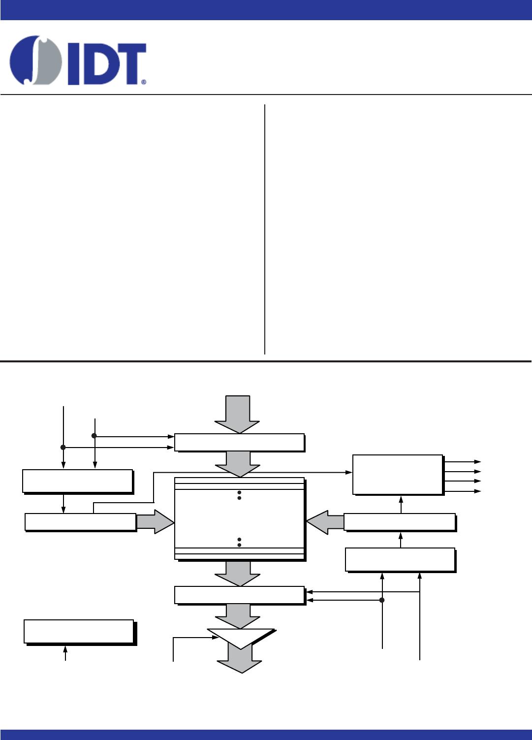
FUNCTIONAL BLOCK DIAGRAM
FEATURES:
••
••
• 64 x 8-bit organization (IDT72420)
••
••
• 256 x 8-bit organization (IDT72200)
••
••
• 512 x 8-bit organization (IDT72210)
••
••
• 1,024 x 8-bit organization (IDT72220)
••
••
• 2,048 x 8-bit organization (IDT72230)
••
••
• 4,096 x 8-bit organization (IDT72240)
••
••
• 10 ns read/write cycle time (IDT72420/72200/72210/72220/72230/
72240)
••
••
• Read and Write Clocks can be asynchronous or coincidental
••
••
• Dual-Ported zero fall-through time architecture
••
••
• Empty and Full flags signal FIFO status
••
••
• Almost-Empty and Almost-Full flags set to Empty+7 and Full-7,
respectively
••
••
• Output enable puts output data bus in high-impedance state
••
••
• Produced with advanced submicron CMOS technology
••
••
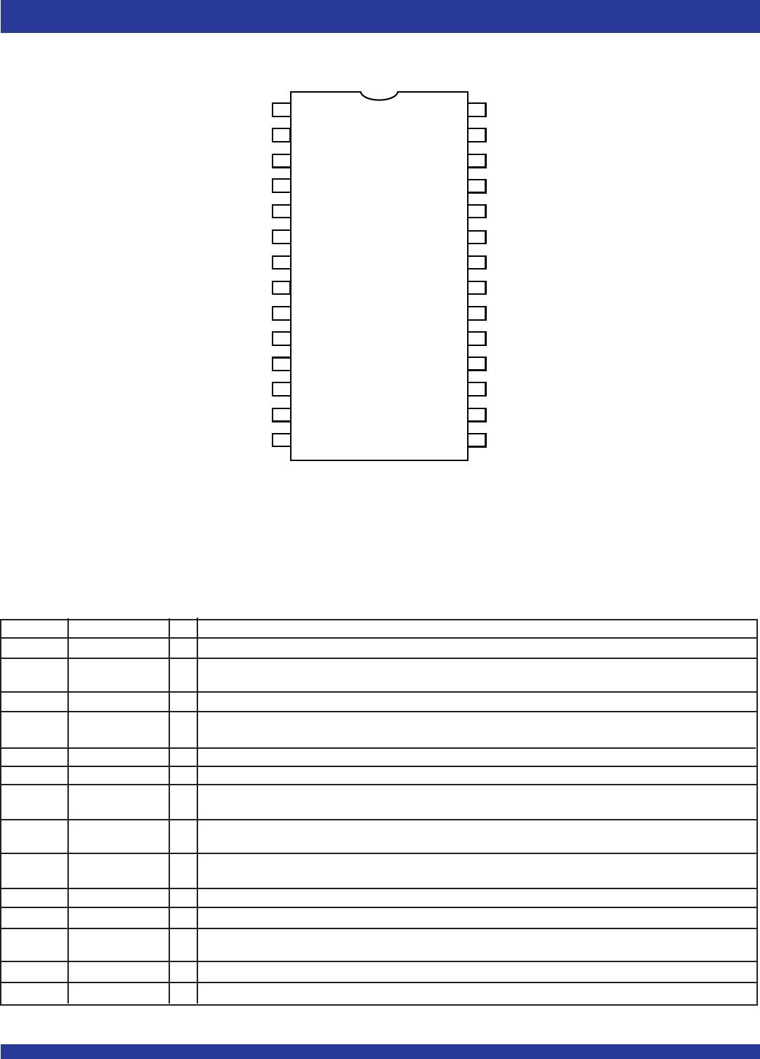
• Available in 28-pin 300 mil plastic DIP
••
••
• For surface mount product please see the IDT72421/72201/72211/
72221/72231/72241 data sheet
••
••
• Green parts available, see ordering information
INPUT REGISTER
OUTPUT REGISTER
RAM ARRAY
64 x 8, 256 x 8,
512 x 8, 1,024 x 8,
2,048 x 8, 4,096 x 8
FLAG
LOGIC
READ POINTER
READ CONTROL
LOGIC
WRITE CONTROL
LOGIC
WRITE POINTER
RESET LOGIC
WCLK
RCLK
REN
D0 - D7
Q0 - Q7
RS
OE
FF
AF
AE
EF
WEN
2680 drw01