LTC4245
24
4245fa
APPLICATIO S I FOR ATIO
WUU
U
SDA line during the acknowledge clock pulse. When the
slave is the receiver, it must pull down the SDA line so that
it remains LOW during this pulse to acknowledge receipt
of the data. If the slave fails to acknowledge by leaving
SDA HIGH, then the master can abort the transmission by
generating a STOP condition. When the master is receiving
data from the slave, the master must pull down the SDA
line during the clock pulse to indicate receipt of the data.
After the last byte has been received, the master will leave
the SDA line HIGH (not acknowledge) and issue a STOP
condition to terminate the transmission.
Write Protocol
The master begins communication with a START condition
followed by the seven bit slave address and the R/
⎯
W bit set
to zero. The addressed LTC4245 acknowledges this and
then the master sends a command byte which indicates
which internal register the master wishes to write. The
LTC4245 acknowledges this and then latches the lower
fi ve bits of the command byte into its internal Register
Address Pointer. The master then delivers the data byte
and the LTC4245 acknowledges once more and latches the
data into its internal register. The transmission is ended
when the master sends a STOP condition. If the master
continues sending a second data byte, as in a Write Word
command, the second data byte will be acknowledged by
the LTC4245 but ignored.
Read Protocol
The master begins a read operation with a START condition
followed by the seven bit slave address and the R/
⎯
W bit set
to zero. The addressed LTC4245 acknowledges this and
then the master sends a command byte which indicates
which internal register the master wishes to read. The
LTC4245 acknowledges this and then latches the lower
fi ve bits of the command byte into its internal Register
Address Pointer. The master then sends a repeated START
condition followed by the same seven bit address with the
R/
⎯
W bit now set to one. The LTC4245 acknowledges and
sends the contents of the requested register. The transmis-
sion is ended when the master sends a STOP condition.
If the master acknowledges the transmitted data byte, as
in a Read Word command, the LTC4245 will repeat the
requested register as the second data byte.
Note that the Register Address Pointer is not cleared at
the end of the transaction. Thus the Receive Byte protocol
can be used to repeatedly read a specifi c register.
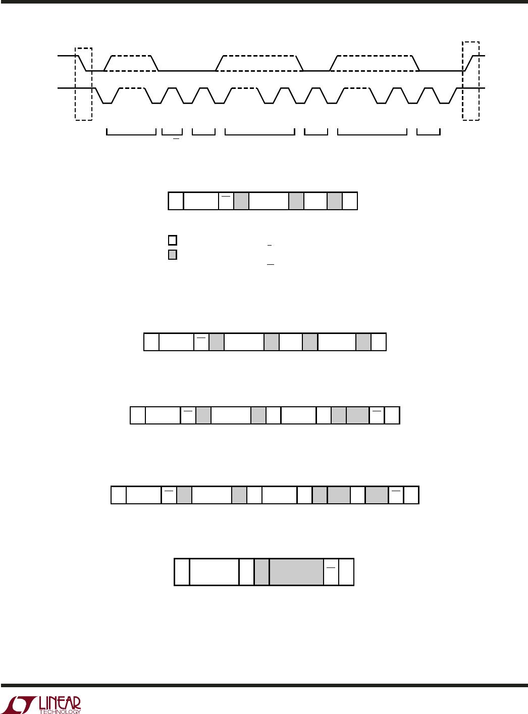
Alert Response Protocol
The LTC4245 implements the SMBus Alert Response Pro-
tocol as shown in Figure 16. If enabled to do so through
the ALERT register B, the LTC4245 will respond to faults
by pulling the ALERT# pin low. Multiple LTC4245s can
share a common ALERT# line and the protocol allows a
master to determine which LTC4245s are pulling the line
low. The master begins by sending a START bit followed
by the special Alert Response Address (0001 100)b with
the R/
⎯
W bit set to one. Any LTC4245 that is pulling its
ALERT# pin low will acknowledge and begin sending back
its individual slave address.
An arbitration scheme ensures that the LTC4245 with the
lowest address will have priority; all others will abort their
response. The successful responder will then release its
ALERT# pin while any others will continue to hold their
ALERT# pins low. Polling may also be used to search for any
LTC4245 that have detected faults. Any LTC4245 pulling its
ALERT# pin low will have bit B3 in the ALERT register set.
Writing a zero to this bit will release the ALERT# pin.
The ALERT# signal will not be pulled low again until the
FAULT1 or FAULT2 register indicates a different fault has
occurred or the original fault is cleared and it occurs again.
Note that this means repeated or continuing faults will not
generate alerts until the associated fault register bit has
been cleared. Also, a fault on one supply will not gener-
ate an alert if a fault bit of the same kind (undervoltage,
overcurrent, power bad) is set for any other supply.
General Purpose Input/Outputs (GPIOs)
The G36 package of the LTC4245 has one GPIO (GPIO1)
pin while the UHF package has three (GPIO1 to GPIO3). Bits
G0 to G2 in the GPIO register (Table 13) indicate whether
a pin is above or below the 1V threshold voltage. Bits G3
to G5 control whether the open-drain output on a GPIO
pin pulls low or is high impedance. This can be used to
drive external pull-up resistors or LEDs. Register bits G6
and G7 control which one of the three pins is multiplexed
to the GPIO channel of the ADC. Whenever the GPIO1 pin