LTC4245
25
4245fa
toggles, bit F7 is set to indicate a change of state. If the
GPIO1 alert bit B7 is enabled, this feature can be used to
alert the host system to a change in state of the board’s
ejector handles.
Compensating the Active Current Loop
The four active current limit circuits of the LTC4245 are
compensated internally and therefore do not require any
RC network on the gate pins. The internal compensation
should work for most pass transistors. If the gate capaci-
tance is very small then the best method to compensate
the loop is to add a 1nF to 5nF capacitor between the gate
and source of the external MOSFET.
Supply Collapse During Transients
The LTC4245 is designed to ride through supply transients
caused by load steps. If there is a shorted load and the
parasitic inductance back to the supply is signifi cant, there
is a chance that the supply could collapse before the active
current limit circuit brings down the gate of the external
MOSFET. In this case the undervoltage lockout circuit,
which has a 3.5μs (5.5μs for V
EEIN
) fi lter time, turns off
the pass transistors.
Input Overvoltage Transient Protection
Hot-plugging a board into a backplane generates inrush
currents from the backplane power supplies due to the
charging of the plug-in board capacitance. To reduce this
transient current to a safe level, the CPCI Hot Swap speci-
cation restricts the amount of unswitched capacitance
used on the input side of the plug-in board. Each medium
or long power pin connected to the CPCI female connector
on the plug-in board is required to have a 10nF ceramic
bypass capacitor to ground. Bulk capacitors are allowed
on the switched output side of the LTC4245. Some bulk
capacitance is allowed on the Early Power planes, but only
because a current limiting resistor is assumed to decouple
the connector pin from the bulk capacitance (e.g., see
100Ω to Bus Switch V
DD
in Figure 10).
Disallowing bulk capacitors on the input power pins tends
to create a resonant circuit formed by the inductance of
the backplane power supply trace and the parasitic capaci-
tance of the plug-in board (mainly due to the large power
MOSFET). Upon board insertion, the ringing of this circuit
can exhibit a peak overshoot of 2.5 times the steady-state
voltage (>30V for 12V
IN
).
There are two methods for abating the effects of these
high voltage transients: using voltage limiters to clip the
transient to a safe level and snubber networks. Snubber
networks are series RC networks whose time constants are
experimentally determined based on the board’s parasitic
resonance circuits. As a starting point, the capacitors in
these networks are chosen to be 10× to 100× the power
MOSFET’s C
OSS
under bias. The series resistor is a value
determined experimentally that ranges from 1Ω to 50Ω,
depending on the parasitic resonance circuit. Note that
in all LTC4245 circuit schematics, both transient voltage
limiters and snubber networks have been added to the
12V
IN
and V
EEIN
supply rails and should always be used.
Snubber networks are not necessary on the 3V
IN
or the
5V
IN
supply lines since their absolute maximum ratings are
10V. Transient voltage limiters, however, are recommended
as these devices provide large-scale transient protection
for the LTC4245 in the event of abrupt changes in supply
current. All protection networks should be mounted very
close to the LTC4245’s supply pins using short lead lengths
to minimize the trace resistance and inductance. A rec-
ommended layout of the 5V and 12V transient protection
devices around the LTC4245 is shown in Figure 18.
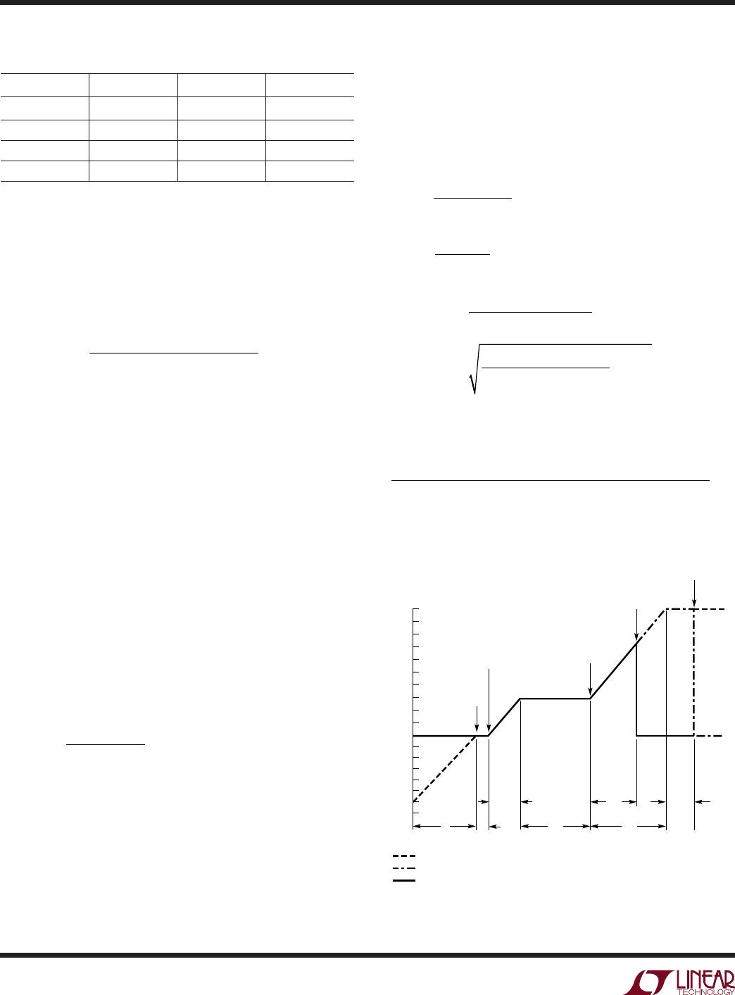
Design Example
As a design example, consider a Hot Swap application
with the following power supply requirements:
Table 1. Example Power Supply Requirements
VOLTAGE
SUPPLY
MAXIMUM
LOAD
CURRENT
MAXIMUM
INRUSH dI/dt
LOAD
CAPACITANCE
12V 600mA 150mA/ms 100μF
5V 5A 1.5A/ms 2200μF
3.3V 7A 1.5A/ms 2200μF
–12V 300mA 150mA/ms 100μF
1. Select the appropriate values of R
SENSE
for the supplies.
Calculating the value of R
SENSE
is based on I
LOAD(MAX)
and the lower limit for the circuit breaker threshold volt-
age, ΔV
SNS(CB)(MIN)
. If a 1% tolerance is assumed for the
sense resistors, then the following values of resistances
should suffi ce:
APPLICATIO S I FOR ATIO
WUU
U
LTC4245
26
4245fa
Table 2. Sense Resistance Values
SUPPLY R
SENSE
(1%) I
TRIP(MIN)
I
TRIP(MAX)
12V 50mΩ 891mA 1.1A
5V 3.5mΩ 6.4A 7.9A
3.3V 2.5mΩ 8.9A 11.1A
–12V 100mΩ 396mA 606mA
If necessary, two resistors with the same tolerance can
be connected in parallel to yield the 3.5mΩ and 2.5mΩ
values.
2. Select the SS capacitor for limiting the rate of rise of
inrush current. Equations 1 and 2 lead to the following
design equation:
C
GI
RdIdt
SS MIN
SS SS MAX
SENSE MIN MA
()
()
() (
•( / )
XX)
(6)
Applying Equation 6 to the 12V supply, with G
SS
of 46mV/V,
I
SS(MAX)
of 24μA, R
SENSE(MIN)
of 49.5mΩ, and (dI/dt)
(MAX)
of 150mA/ms yields a C
SS(MIN)
greater than 149nF. This
capacitance value satisfi es the dI/dt requirements of the
other supplies too. Hence, a 220nF (±10%) capacitor is
chosen for C
SS
.
3. To determine the TIMER capacitance, the time required
to completely power-up all supply outputs simultaneously
needs to be calculated. There are three parts to this time:
time for the internal current limit to cross zero (t
1
), time
for the gate to slew to the MOSFET threshold voltage (t
2
)
and the time for the current fl ow to charge up the load
capacitors (t
3
) (see Figure 17).
t
1
: The time for the internal current limit to rise above
zero is simply:
t
I
dI dt
FBL MIN
MIN
1
4=
(/)
()
()
(7)
t
2
: The maximum time for the gate of the external MOSFET to
rise to the threshold voltage depends on I
GATE(UP)(MIN)
and
the gate charge required to turn on the external MOSFET.
A typical value for this time is 1ms. This can be verifi ed
after the MOSFETs are selected. Since the current limit
ramp is almost stopped while any MOSFET is turning on,
t
2
is 4 times 1ms or 4ms, since in the worst case none of
the four MOSFET turn-ons overlaps in time.
t
3
: Under simultaneous power-up each output voltage af-
fects the inrush current profi le. To simplify calculations, the
inrush current profi le shown in Figure 17 is chosen. All the
current is assumed to charge the load capacitor, i.e., there
is no load current. There are four parts to t
3
as shown.
Equations 8 to 11 are used to determine t
31
to t
34
:
t
I
dI dt
FBL MIN
MIN
31
=
()
()
(/)
(8)
t
CV
I
t
LFB
FBL MIN
32 31
05=
–.
()
(9)
t
II
dI dt
C
FBH MIN FBL MIN
MIN
L
33
2
=min
(/)
,
() ()
()
•( )
(/)
()
VV
dI dt
tt
OUT FB
MIN
+−
2
31 31
(10)
t
CV V t I I
L OUT FB FBL MIN
34
33
0
05
=
+
max
,
•( ) . •(
()FFBH MIN
FBH MIN
I
()
()
)
(11)
APPLICATIO S I FOR ATIO
WUU
U
t
1
t
31
V
GATE
= 0
V
GATE
= V
TH
I
NEG
0
I
FBL
I
FBH
V
OUT
= V
FB
V
OUT
= V
IN
(SMALL C
L
)
V
OUT
= V
IN
(LARGE C
L
)
t
32
t
33
t
33
t
34
OR
t
2
4245 F17
INTERNAL CURRENT LIMIT
INRUSH CURRENT FOR LARGER C
L
INRUSH CURRENT FOR SMALLER C
L
Figure 17. Inrush Current Profi le for Design Example
LTC4245
27
4245fa
The inputs to the above equations are pre-calculated in
Table 3.
Table 3. t
3
Calculation Inputs
SUPPLY V
OUT
V
FB
(dI/dt)
(MIN)
I
FBL(MIN)
I
FBH(MIN)
12V 12V 6V 60mA/ms 198mA 792mA
5V 5V 3V 430mA/ms 1.13A 6.22A
3.3V 3.3V 2V 602mA/ms 1.58A 8.71A
–12V 12V 6V 30mA/ms 109mA 396mA
Equations 8 to 11, when applied to the four supplies
yields:
Table 4. t
3
Calculation Results
SUPPLY t
31
t
32
t
33
t
34
TOTAL(t
3
)
12V 3.3ms 1.4ms 2.3ms 0 7ms
5V 2.6ms 4.5ms 2.6ms 0 9.7ms
3.3V 2.6ms 1.5ms 1.4ms 0 5.5ms
–12V 3.6ms 3.7ms 3.7ms 0 11ms
Therefore the TIMER capacitance value is constrained by
the –12V supply inrush current. The total time (t
1
+ t
2
+
t
3
) is approximately 30ms. Equation 4 gives the capacitor
value to be:
C
T(MIN)
≥ 30ms / K
TMCAP(MIN)
= 1.5μF (12)
So a value of 2.2μF (±10%) should suffi ce.
4. The next step is to select MOSFETs for the four sup-
plies. The IRF7413 is selected for 12V, Si7880DP for 5V
and 3.3V, and Si4872 for –12V Supply. The Si7880DP’s
on resistance is less than 4.25mΩ for V
GS
= 4.5V and a
junction temperature of 25°C.
Since the maximum load current requirement for the
3.3V supply is 7A, the steady-state power the MOSFET
may be required to dissipate is 208mW. The Si7880DP
has a maximum junction-to-ambient thermal resistance
of 65°C/W. If a maximum ambient temperature of 50°C
is assumed, this yields a junction temperature of 63.5°C.
According to the Si7880DP’s Normalized On-Resistance
vs Junction Temperature curve, the device’s on-resistance
can be expected to increase by about 15% over its room
temperature value. Recalculation of the steady-state values
of R
ON
and junction temperature yields approximately
4.9mΩ and 67°C, respectively. The I • R drop across the
3.3V sense resistor and series MOSFET at maximum load
current under these conditions will be less than 52mV.
The energy dissipated in the MOSFET during power-up
is the same as that stored into the load capacitor. The
average power dissipated in the MOSFET is:
P
CV
t
ON
L OUT
=
2
3
2
(13)
The 12V MOSFET’s single-pulse θ
JA(MAX)
, as read from
its Transient Thermal Impedance Graph, is 3°C/W for a
time, t
3
, of 7ms. P
ON
is calculated to be 1W and therefore
the 12V MOSFET temperature rise during power-up is
3°C. The other supplies show a smaller rise in MOSFET
temperature than this value.
When a supply powers-up into a short-circuit at the output,
the supply current rises linearly to the lower foldback level
and stays there till the timer expires and the MOSFETs are
shut-off. To simplify calculations it will be assumed that
the MOSFET conducts the lower foldback current from
the moment it turns on. This time (t
SC
) is the actual time
the MOSFET is conducting current minus a correction
for the assumption, which is half of the time required for
the current to rise from zero to the lower foldback level.
Therefore:
tCK
V
SC MAX T MAX TMCAP MAX
SNS FBL
() () ()
(
•–
(.
=
15
))( ) ( )
()
)•
MAX SS MIN
SS SS MAX
C
GI
(14)
The 1.5 • ΔV
SNS(FBL)(MAX)
term is due to the correction
factor and the time spent in ramping the starting negative
current limit to zero. t
SC(MAX)
turns out to be about 58ms
for all four supplies. The maximum power dissipated in
the MOSFET is given by:
PI V
SC MAX FBL MAX OUT() ()
=
(15)
P
SC(MAX)
for the 5V supply is 3.2A • 5V, or 16W. θ
JA(MAX)
for the 5V MOSFET is 3.25°C/W. Therefore the MOSFET
temperature rise during power-up into a 5V
OUT
short-
circuit is 52°C. Similar calculations show that the other
supplies experience a smaller MOSFET temperature rise.
The θ
JA(MAX)
value is read from the MOSFET datasheet’s
Transient Thermal Impedance Graph for a duty cycle of
0.02, which is the case when the LTC4245 is confi gured
for auto-retry on overcurrent faults.
APPLICATIO S I FOR ATIO
WUU
U

LTC4245IG#PBF

Mfr. #:
Manufacturer:
Analog Devices Inc.
Description:
Hot Swap Voltage Controllers Quad Hot Swap Contr. w/ADC and I2C
Lifecycle:
New from this manufacturer.
Delivery:
DHL FedEx Ups TNT EMS
Payment:
T/T Paypal Visa MoneyGram Western Union