LTC4245
28
4245fa
drop and temperature rise to a minimum, the suggested
trace width in these applications for 1oz copper foil is
0.03” for each ampere of DC current.
In the majority of applications, it will be necessary to use
plated-through vias to make circuit connections from
component layers to power and ground layers internal
to the PCB. For 1oz copper foil plating, a general rule is
1A of DC current per via, making sure the via is properly
dimensioned so that solder completely fi lls any void. For
other plating thicknesses, check with your PCB fabrica-
tion facility.
It is also important to put C1, the bypass capacitor for the
INTV
CC
pin as close as possible between INTV
CC
and GND.
The surge suppressors, Z1 and Z2, are placed between the
supply inputs and ground using wide traces.
PCB Layout Considerations
For proper operation of the LTC4245’s circuit breaker,
Kelvin connection to the sense resistors is strongly
recommended. The PCB layout should be balanced and
symmetrical to minimize wiring errors. In addition, the
PCB layout for the sense resistors and the power MOSFETs
should include good thermal management techniques for
optimal device power dissipation. A recommended PCB
layout for the 5V sense resistor and the power MOSFET
around the LTC4245 is illustrated in Figure 18. In Hot Swap
applications where load currents can be 10A, narrow PCB
tracks exhibit more resistance than wider tracks and operate
at more elevated temperatures. Since the sheet resistance
of 1 ounce copper foil is approximately 0.5mΩ/o, track
resistances and voltage drops add up quickly in high current
applications. Thus, to keep PCB track resistance, voltage
APPLICATIO S I FOR ATIO
WUU
U
Figure 18. Recommended Layout for R2, Q2, R6, Z2, C1, Z1, R10 and C2
1
2
3
4
5
6
7
8
9
10
36
35
34
33
32
31
30
29
28
27
LTC4245G*
CURRENT FLOW
TO SOURCE
*ADDITIONAL DETAILS OMITTED FOR CLARITY
DRAWING IS NOT TO SCALE!
4245 F18
TRACK WIDTH W:
0.03" PER AMPERE
ON 1 OZ Cu FOIL
D
D
D
D
G
S
S
S
CURRENT FLOW
TO LOAD
CURRENT FLOW
TO LOAD
R2 SENSE
RESISTOR
Q2
SO-8
VIA TO
GND PLANE
VIA TO
GND PLANE
GND
GND
GND
5V
OUT
5V
IN
R10
C2
R6
5V
IN
12
VIN
5V
SENSE
5V
GATE
5V
OUT
INTV
CC
WW
W
Z2
Z1
C1
LTC4245
29
4245fa
Table 5. LTC4245 I
2
C Device Addressing
DESCRIPTION
HEX DEVICE
ADDRESS BINARY DEVICE ADDRESS LTC4245 ADDRESS PINS*
H 6 543210 R/
W ADR3 ADR2 ADR1 ADR0
Mass Write 2E 0 0 1 0 1 1 1 0 XXXX
Alert Response 19 0 0 0 1 1 0 0 1 XXXX
0 40 0100000X LLLL
1 42 0 100001 X L L L NC
2 44 0100010X L LNCL
3 46 0 100011 X L L NC NC
4 48 0 100100 X L NC L L
5 4A 0 100101 X L NC L NC
6 4C 0 1 0 0 1 1 0 X L NC NC L
7 4E 0 1 0 0 1 1 1 X L NC NC NC
8 50 0 101000 X NC L L L
9 52 0101001X NCL LNC
10 54 0101010X NCLNCL
11 56 0 1 0 1 0 1 1 X NC L NC NC
12 58 0 1 0 1 1 0 0 X NC NC L L
13 5A 0 1 0 1 1 0 1 X NC NC L NC
14 5C 0 1 0 1 1 1 0 X NC NC NC L
15 5E 0101111 X NCNCNCNC
16 60 0 1 1 0 0 0 0 X L H L L
17 62 0 1 1 0 0 0 1 X L H L NC
18 64 0 1 1 0 0 1 0 X L H NC L
19 66 0 1 1 0 0 1 1 X L H NC NC
20 68 0 1 1 0 1 0 0 X NC/H H L L
21 6A 0 1 1 0 1 0 1 X NC/H H L NC
22 6C 0 1 1 0 1 1 0 X NC/H H NC L
23 6E 0 1 1 0 1 1 1 X NC/H H NC NC
24 70 0 1 1 1 0 0 0 X H L L L
25 72 0 1 1 1 0 0 1 X H L L NC
26 74 0 1 1 1 0 1 0 X H L NC L
27 76 0 1 1 1 0 1 1 X H L NC NC
28 78 0 1 1 1 1 0 0 X H NC L L
29 7A 0 1 1 1 1 0 1 X H NC L NC
30 7C 0 1 1 1 1 1 0 X H NC NC L
31 7E 0 1 1 1 1 1 1 X H NC NC NC
* L = Low, H = High, NC = Not Connected, X = Don’t Care
APPLICATIO S I FOR ATIO
WUU
U
LTC4245
30
4245fa
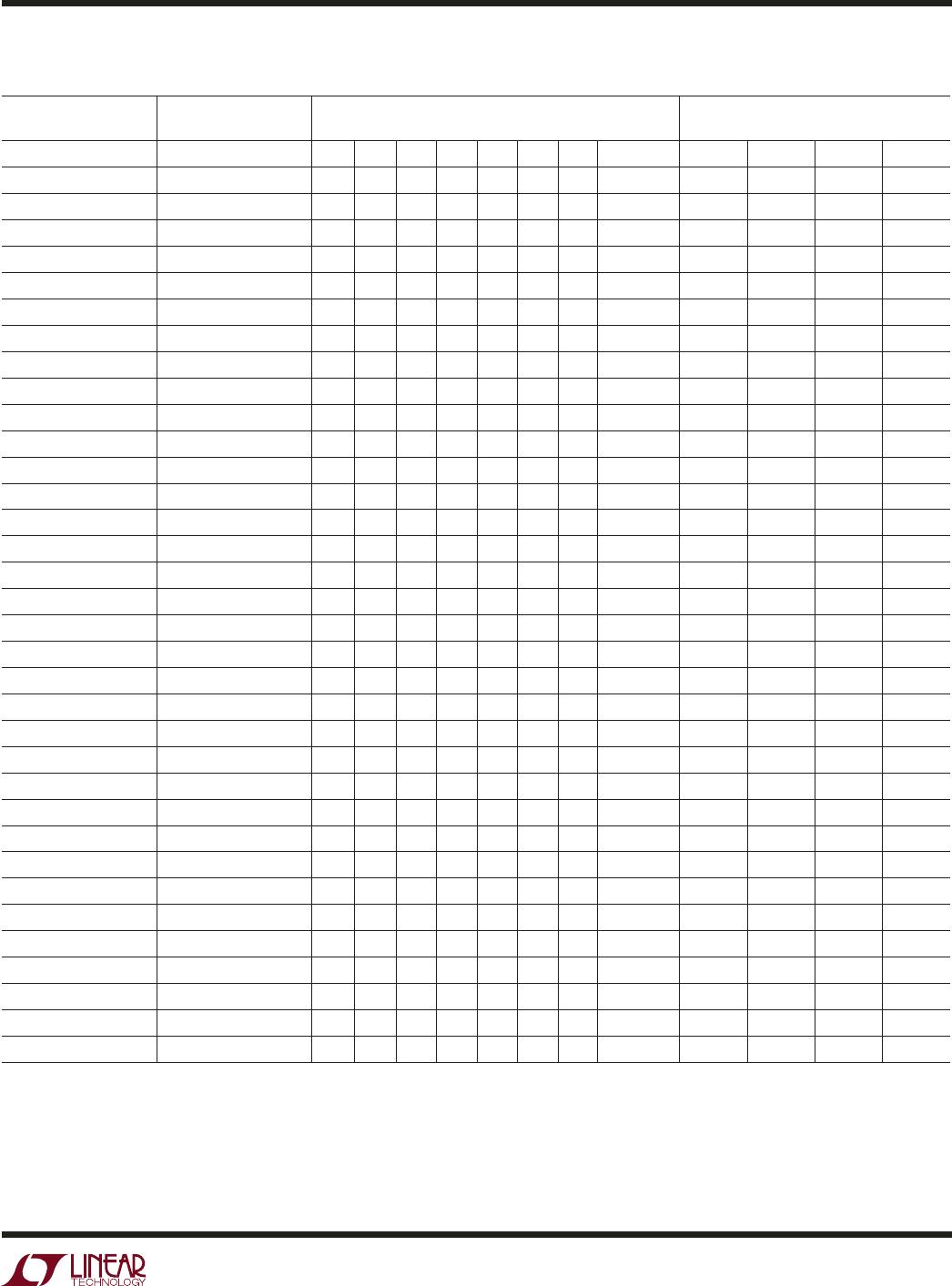
Table 6. LTC4245 Register Address and Contents
REGISTER ADDRESS* REGISTER NAME READ/WRITE DESCRIPTION
DECIMAL HEX
0, 8 00h, 08h STATUS (A) R System Status Information
1, 9 01h, 09h ALERT (B) R/W Controls Which Faults Cause ALERT# Pin to be Pulled Low
2, 10 02h, 0Ah CONTROL (C) R/W Controls Part Behavior Such As Auto-Retry, Sequencing, etc.
3, 11 03h, 0Bh ON (D) D3:D0 R/W**, D7:D4 R Sets State and Reports Status of Switches
4, 12 04h, 0Ch FAULT1 (E) R/W Fault Log for Undervoltage and Overcurrent
5, 13 05h, 0Dh FAULT2 (F) R/W Fault Log for Power Bad, PGI, FET Short, BD_SEL#, GPIO1
6, 14 06h, 0Eh GPIO (G) G2:G0 R, G7:G3 R/W Sets State and Reports Status of GPIO1 to GPIO3 pins, Control
Which Pin is Multiplexed to the GPIO Channel of ADC
7, 15 07h, 0Fh ADCADR (H) R/W 4-Bit ADC Channel Address for On-Demand ADC Measurement
16 10h 12VIN (I) R/W
ADC 12V
IN
Voltage Data
17 11h 12VSENSE (J) R/W
ADC 12V Current Sense Voltage Data
18 12h 12VOUT (K) R/W
ADC 12V
OUT
Voltage Data
19 13h 5VIN (L) R/W
ADC 5V
IN
Voltage Data
20 14h 5VSENSE (M) R/W
ADC 5V Current Sense Voltage Data
21 15h 5VOUT (N) R/W
ADC 5V
OUT
Voltage Data
22 16h 3VIN (O) R/W
ADC 3V
IN
Voltage Data
23 17h 3VSENSE (P) R/W
ADC 3.3V Current Sense Voltage Data
24 18h 3VOUT (Q) R/W
ADC 3V
OUT
Voltage Data
25 19h VEEIN (R) R/W
ADC V
EEIN
Voltage Data
26 1Ah VEESENSE (S) R/W
ADC –12V Current Sense Voltage Data
27 1Bh VEEOUT (T) R/W
ADC V
EEOUT
Voltage Data
28 to 31 1Ch to 1Fh GPIOADC (U) R/W
ADC GPIO Voltage Data
All registers are 8-bit wide.
* Register address MSBs b7 – b5 are ignored.
** Cannot set D3:D0 high if bit A1 set.
Set bit C7 before writing.
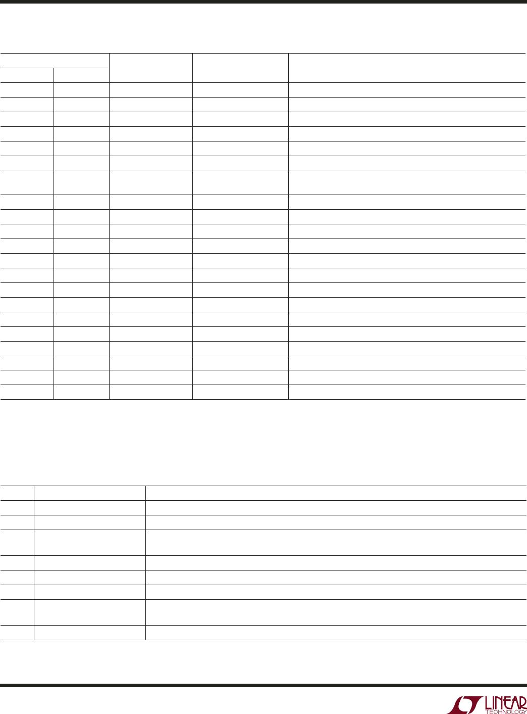
Table 7. STATUS Register A (00h)- Read Only
BIT NAME OPERATION
A7 ADC Busy Indicates State of ADC; 1 = ADC Busy Measuring, 0 = ADC Quiescent
A6 BD_SEL# Input State of the BD_SEL# Pin; 1 =BD_SEL# High, 0 = BD_SEL# Low
A5 FET Short Present Indicates Potential FET Short on at Least One Supply, if ADC Current Sense Voltage Measurement Exceeds 7
LSB While FET is Off; 1 = FET is Shorted, 0 = FET is Not Shorted
A4 LOCAL_PCI_RST# Output LOCAL_PCI_RST# Pin Open-Drain Output State; 1 = High Impedance, 0 = Pulls Low
A3 PCI_RST# Input State of the PCI_RST# Pin; 1 = PCI_RST# High, 0 = PCI_RST# Low
A2 Power Bad Indicates Power Bad Present on at Least One of the Supply Outputs; 1 = Power Bad, 0 = No Power Bad
A1 SS Busy Indicates SS Pin is Being Used to Ramp Up a Supply, Affects Writing to D3:D0 Bits
1 = SS Pin Ramping, Cannot Set D3:D0 High, 0 = SS Pin Reset
A0 Undervoltage Indicates Undervoltage Present on at Least One of the Input Supply; 1 = Undervoltage, 0 = Not Undervoltage
APPLICATIO S I FOR ATIO
WUU
U

LTC4245IG#PBF

Mfr. #:
Manufacturer:
Analog Devices Inc.
Description:
Hot Swap Voltage Controllers Quad Hot Swap Contr. w/ADC and I2C
Lifecycle:
New from this manufacturer.
Delivery:
DHL FedEx Ups TNT EMS
Payment:
T/T Paypal Visa MoneyGram Western Union