© 2008 Microchip Technology Inc. DS22116A-page 1
24VL014H
Device Selection Table
Features:
• Single-Supply with Operation Down to 1.5V
• Low-Power CMOS Technology:
- 400 μA active current, maximum
-1 μA standby current, maximum
• 2-Wire Serial Interface Bus, I
2
C™ Compatible
• Schmitt Trigger Inputs for Noise Suppression
• Output Slope Control to Eliminate Ground Bounce
• 100 kHz and 400 kHz Compatibility
• Page Write Buffer for up to 16 Bytes
• Self-Timed Write Cycle (including Auto-Erase)
• Hardware Write Protection for Half Array
(40h-7Fh)
• Cascadable up to Eight Devices
• More than 1 Million Erase/Write Cycles
• ESD Protection > 4,000V
• Data Retention > 200 Years
• Factory Programming (QTP) Available
• 8-pin PDIP, SOIC, TSSOP, TDFN and MSOP
Packages
• Temperature Range:
• Pb-Free and RoHS Compliant
Description:
The Microchip Technology Inc. 24VL014H is a 1 Kbit
Serial Electrically Erasable PROM with operation
down to 1.5V. The device is organized as a single block
of 128 x 8-bit memory with a 2-wire serial interface.
Low-current design permits operation with maximum
standby and active currents of only 1 μA and 400 μA,
respectively. The device has a page write capability for
up to 16 bytes of data. Functional address lines allow
the connection of up to eight 24VL014H devices on the
same bus for up to 8 Kbits of contiguous EEPROM
memory. The device is available in the standard 8-pin
PDIP, 8-pin SOIC (150 mil), TSSOP, 2x3 TDFN and
MSOP packages.
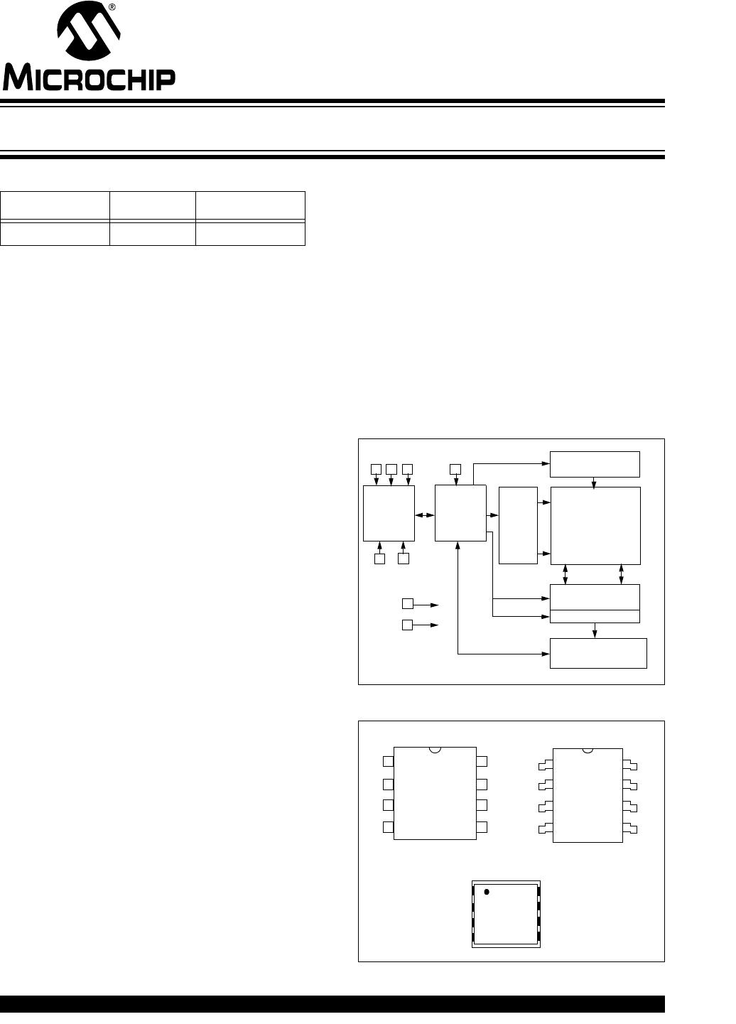
Block Diagram
Package Types
Part Number VCC Range Max Clock
24VL014H 1.5 to 3.6V 400 kHz
(1)
Note 1: 100 kHz for VCC < 1.8V
- -20°C to +85°C
I/O
Control
Logic
Memory
Control
Logic
XDEC
HV Generator
EEPROM
Array
Write-Protect
Circuitry
YDEC
V
CC
VSS
Sense Amp.
R/W Control
SDA
SCL
A0 A1 A2
WP
A0
A1
A2
V
SS
VCC
WP
SCL
SDA
1
2
3
4
8
7
6
5
PDIP, MSOP
SOIC, TSSOP
A0
A1
A2
V
SS
1
2
3
4
8
7
6
5
V
CC
WP
SCL
SDA
TDFN
A0
A1
A2
V
SS
WP
SCL
SDA
V
CC
8
7
6
5
1
2
3
4
1K I
2
C
™
Serial EEPROM with Half-Array Write-Protect