© 2008 Microchip Technology Inc. DS22116A-page 9
24VL014H
6.0 WRITE OPERATIONS
6.1 Byte Write
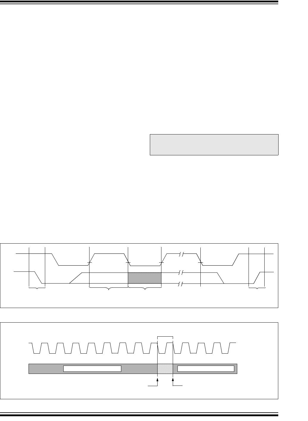
Following the Start signal from the master, the device
code (4 bits), the Chip Select bits (3 bits) and the R/W
bit (which is a logic low) are placed onto the bus by the
master transmitter. The device will acknowledge this
control byte during the ninth clock pulse. The next byte
transmitted by the master is the word address and will
be written into the Address Pointer of the 24VL014H.
After receiving another Acknowledge signal from the
24VL014H, the master device will transmit the data
word to be written into the addressed memory location.
The 24VL014H acknowledges again and the master
generates a Stop condition. This initiates the internal
write cycle and the 24VL014H will not
generate Acknowledge signals during this time
(Figure 6-1). If an attempt is made to write to the
protected portion of the array when the hardware write
protection has been enabled, the device will
acknowledge the command, but no data will be written.
The write cycle time must be observed even if write
protection is enabled.
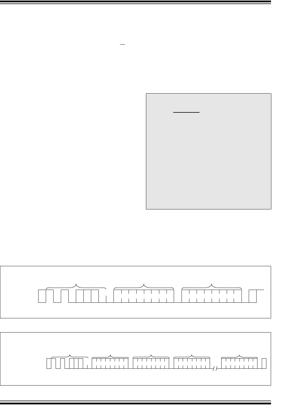
6.2 Page Write
The write-control byte, word address and the first data
byte are transmitted to the 24VL014H in the same way
as in a byte write. But instead of generating a Stop
condition, the master transmits up to 15 additional data
bytes to the 24VL014H that are temporarily stored in
the on-chip page buffer and will be written into the
memory once the master has transmitted a Stop
condition. Upon receipt of each word, the four lower
order Address Pointer bits are internally incremented
by one.
The higher order three bits of the word address remain
constant. If the master should transmit more than 16
bytes prior to generating the Stop condition, the
address counter will roll over and the previously
received data will be overwritten. As with the byte write
operation, once the Stop condition is received, an
internal write cycle will begin (Figure 6-2). If an attempt
is made to write to the protected portion of the array
when the hardware write protection has been enabled,
the device will acknowledge the command, but no data
will be written. The write cycle time must be observed
even if write protection is enabled.
6.3 Write Protection
The WP pin must be tied to VCC or VSS. If tied to VCC,
half of the array will be write-protected (40h-7Fh). If the
WP pin is tied to V
SS, write operations to all address
locations are allowed.
FIGURE 6-1: BYTE WRITE
FIGURE 6-2: PAGE WRITE
Note: Page write operations are limited to writing
bytes within a single physical page,
regardless
of the number of bytes
actually being written. Physical page
boundaries start at addresses that are
integer multiples of the page buffer size (or
‘page size’) and end at addresses that are
integer multiples of [page size – 1]. If a
Page Write command attempts to write
across a physical page boundary, the
result is that the data wraps around to the
beginning of the current page (overwriting
data previously stored there), instead of
being written to the next page, as might be
expected. It is therefore necessary that the
application software prevent page write
operations that would attempt to cross a
page boundary.
S P
Bus Activity
Master
SDA Line
Bus Activity
S
T
A
R
T
S
T
O
P
Control
Byte
Word
Address
Data
A
C
K
A
C
K
A
C
K
S P
Bus Activity
Master
SDA Line
Bus Activity
S
T
A
R
T
Control
Byte
Word
Address (n)
Data (n) Data (n + 15)
S
T
O
P
A
C
K
A
C
K
A
C
K
A
C
K
A
C
K
Data (n +1)