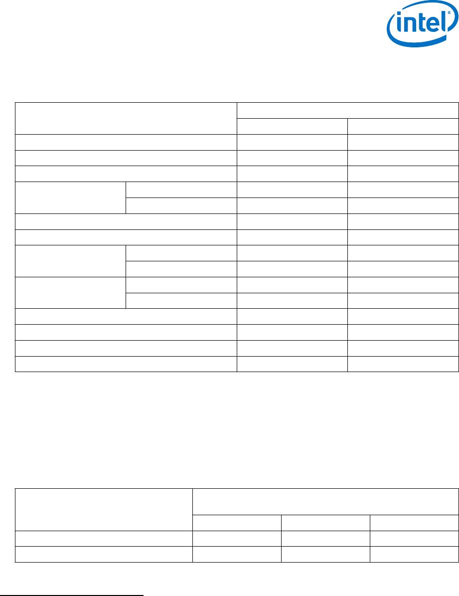
Maximum Resources
Table 10. Maximum Resource Counts for Intel Arria 10 GT Devices
Resource Product Line
GT 900 GT 1150
Logic Elements (LE) (K) 900 1,150
ALM 339,620 427,200
Register 1,358,480 1,708,800
Memory (Kb) M20K 48,460 54,260
MLAB 9,386 12,984
Variable-precision DSP Block 1,518 1,518
18 x 19 Multiplier 3,036 3,036
PLL Fractional Synthesis 32 32
I/O 16 16
Transceiver 17.4 Gbps 72
(5)
72
(5)
25.8 Gbps 6 6
GPIO
(6)
624 624
LVDS Pair
(7)
312 312
PCIe Hard IP Block 4 4
Hard Memory Controller 16 16
Related Information
Intel Arria 10 GT Channel Usage
Configuring GT/GX channels in Intel Arria 10 GT devices.
Package Plan
Table 11. Package Plan for Intel Arria 10 GT Devices
Refer to I/O and High Speed I/O in Intel Arria 10 Devices chapter for the number of 3 V I/O, LVDS I/O, and
LVDS channels in each device package.
Product Line
SF45
(45 mm × 45 mm, 1932-pin FBGA)
3 V I/O LVDS I/O XCVR
GT 900 624 72
GT 1150 624 72
(5)
If all 6 GT channels are in use, 12 of the GX channels are not usable.
(6)
The number of GPIOs does not include transceiver I/Os. In the Intel Quartus Prime software,
the number of user I/Os includes transceiver I/Os.
(7)
Each LVDS I/O pair can be used as differential input or output.
Intel
®
Arria
®
10 Device Overview
A10-OVERVIEW | 2018.04.09
Intel
®
Arria
®
10 Device Overview
13
Related Information
I/O and High-Speed Differential I/O Interfaces in Intel Arria 10 Devices chapter, Intel
Arria 10 Device Handbook
Provides the number of 3 V and LVDS I/Os, and LVDS channels for each Intel Arria
10 device package.
Intel Arria 10 SX
This section provides the available options, maximum resource counts, and package
plan for the Intel Arria 10 SX devices.
The information in this section is correct at the time of publication. For the latest
information and to get more details, refer to the Intel FPGA Product Selector.
Related Information
Intel FPGA Product Selector
Provides the latest information on Intel products.
Available Options
Figure 3. Sample Ordering Code and Available Options for Intel Arria 10 SX Devices
Family Signature
Transceiver Count
Transceiver
Speed Grade
Package Type
Package Code
Operating Temperature
FPGA Fabric
Speed Grade
Optional Suffix
Indicates specific device
options or shipment method
S : SX variant
(SoC with 17.4 Gbps transceivers)
10A : Intel Arria 10
016 : 160K logic elements
022 : 220K logic elements
027 : 270K logic elements
032 : 320K logic elements
048 : 480K logic elements
057 : 570K logic elements
066 : 660K logic elements
K : 36
N : 48
C : 6
E : 12
H : 24
1 (fastest)
2
3
4
F : FineLine BGA (FBGA), 1.0 mm pitch
U : Ultra FineLine BGA (UBGA), 0.8 mm pitch
FBGA Package Type
27 : 672 pins, 27 mm x 27 mm
29 : 780 pins, 29 mm x 29 mm
34 : 1,152 pins, 35 mm x 35 mm
35 : 1,152 pins, 35 mm x 35 mm
40 : 1,517 pins, 40 mm x 40 mm
UBGA Package Type
19 : 484 pins, 19 mm x 19 mm
I :
E :
M :
1 (fastest)
2
3
Power Option
S : Standard
L : Low
RoHS
G : RoHS6
N : RoHS5
P : Leaded
ES : Engineering sample
10A
S F
066
K
2
S35 I
2
ESG
Logic Density
Family Variant
}
Contact Intel
for availability
Industrial (T
J
= -40° C to 100° C)
Extended (T
J
= 0° C to 100° C)
Military (T
J
= -55° C to 125° C)
V
:
SmartVID (Speed Grade -2 and -3 only)
Related Information
Transceiver Performance for Intel Arria 10 GX/SX Devices
Provides more information about the transceiver speed grade.
Intel
®
Arria
®
10 Device Overview
A10-OVERVIEW | 2018.04.09
Intel
®
Arria
®
10 Device Overview
14
Maximum Resources
Table 12. Maximum Resource Counts for Intel Arria 10 SX Devices
Resource Product Line
SX 160 SX 220 SX 270 SX 320 SX 480 SX 570 SX 660
Logic Elements (LE) (K) 160 220 270 320 480 570 660
ALM 61,510 80,330 101,620 119,900 183,590 217,080 251,680
Register 246,040 321,320 406,480 479,600 734,360 868,320 1,006,720
Memory (Kb) M20K 8,800 11,740 15,000 17,820 28,620 36,000 42,620
MLAB 1,050 1,690 2,452 2,727 4,164 5,096 5,788
Variable-precision DSP Block 156 192 830 985 1,368 1,523 1,687
18 x 19 Multiplier 312 384 1,660 1,970 2,736 3,046 3,374
PLL Fractional
Synthesis
6 6 8 8 12 16 16
I/O 6 6 8 8 12 16 16
17.4 Gbps Transceiver 12 12 24 24 36 48 48
GPIO
(8)
288 288 384 384 492 696 696
LVDS Pair
(9)
120 120 168 168 174 324 324
PCIe Hard IP Block 1 1 2 2 2 2 2
Hard Memory Controller 6 6 8 8 12 16 16
ARM Cortex-A9 MPCore
Processor
Yes Yes Yes Yes Yes Yes Yes
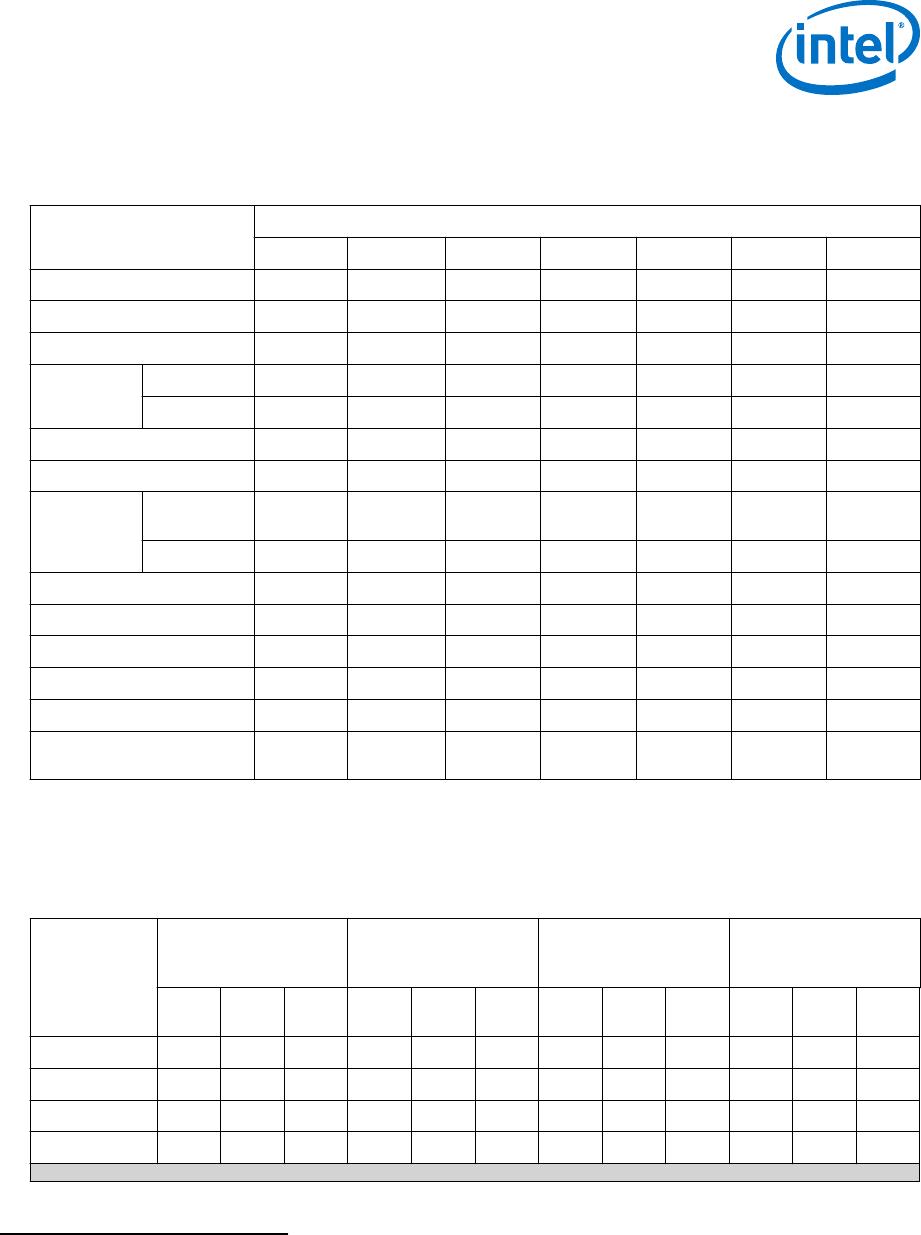
Package Plan
Table 13. Package Plan for Intel Arria 10 SX Devices (U19, F27, F29, and F34)
Refer to I/O and High Speed I/O in Intel Arria 10 Devices chapter for the number of 3 V I/O, LVDS I/O, and
LVDS channels in each device package.
Product Line
U19
(19 mm × 19 mm,
484-pin UBGA)
F27
(27 mm × 27 mm,
672-pin FBGA)
F29
(29 mm × 29 mm,
780-pin FBGA)
F34
(35 mm × 35 mm,
1152-pin FBGA)
3 V
I/O
LVDS
I/O
XCVR 3 V
I/O
LVDS
I/O
XCVR 3 V
I/O
LVDS
I/O
XCVR 3 V
I/O
LVDS
I/O
XCVR
SX 160 48 144 6 48 192 12 48 240 12
SX 220 48 144 6 48 192 12 48 240 12
SX 270 48 192 12 48 312 12 48 336 24
SX 320 48 192 12 48 312 12 48 336 24
continued...
(8)
The number of GPIOs does not include transceiver I/Os. In the Intel Quartus Prime software,
the number of user I/Os includes transceiver I/Os.
(9)
Each LVDS I/O pair can be used as differential input or output.
Intel
®
Arria
®
10 Device Overview
A10-OVERVIEW | 2018.04.09
Intel
®
Arria
®
10 Device Overview
15

10AX115H2F34E1SG

Mfr. #:
Manufacturer:
Intel / Altera
Description:
FPGA - Field Programmable Gate Array
Lifecycle:
New from this manufacturer.
Delivery:
DHL FedEx Ups TNT EMS
Payment:
T/T Paypal Visa MoneyGram Western Union