2001 Nov 07 2
NXP Semiconductors Product data sheet
NPN/PNP general purpose transistor BC847BVN
FEATURES
• 300 mW total power dissipation
• Very small 1.6 mm x 1.2 mm ultra thin package
• Excellent coplanarity due to straight leads
• Replaces two SC-75/SC-89 packaged transistors on
same PCB area
• Reduced required PCB area
• Reduced pick and place costs.
APPLICATIONS
• General purpose switching and amplification
• Switch mode power supply complementary MOSFET
driver
• Complementary driver for audio amplifiers.
DESCRIPTION
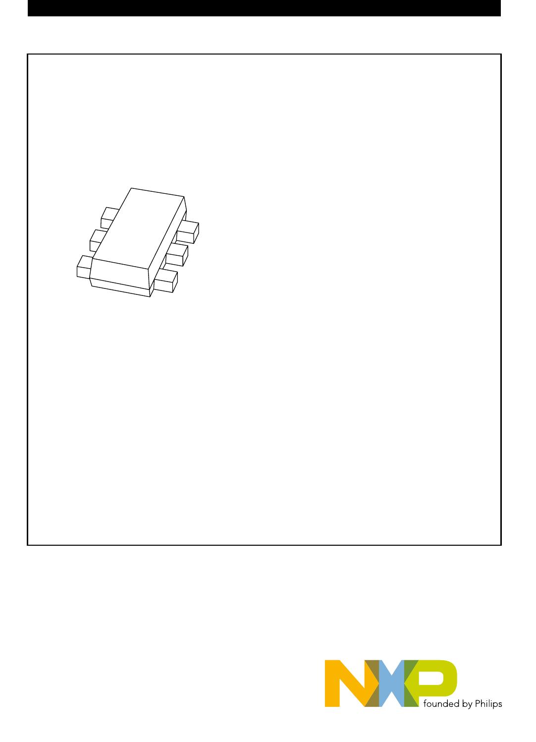
NPN/PNP transistor pair in a SOT666 plastic package.
MARKING
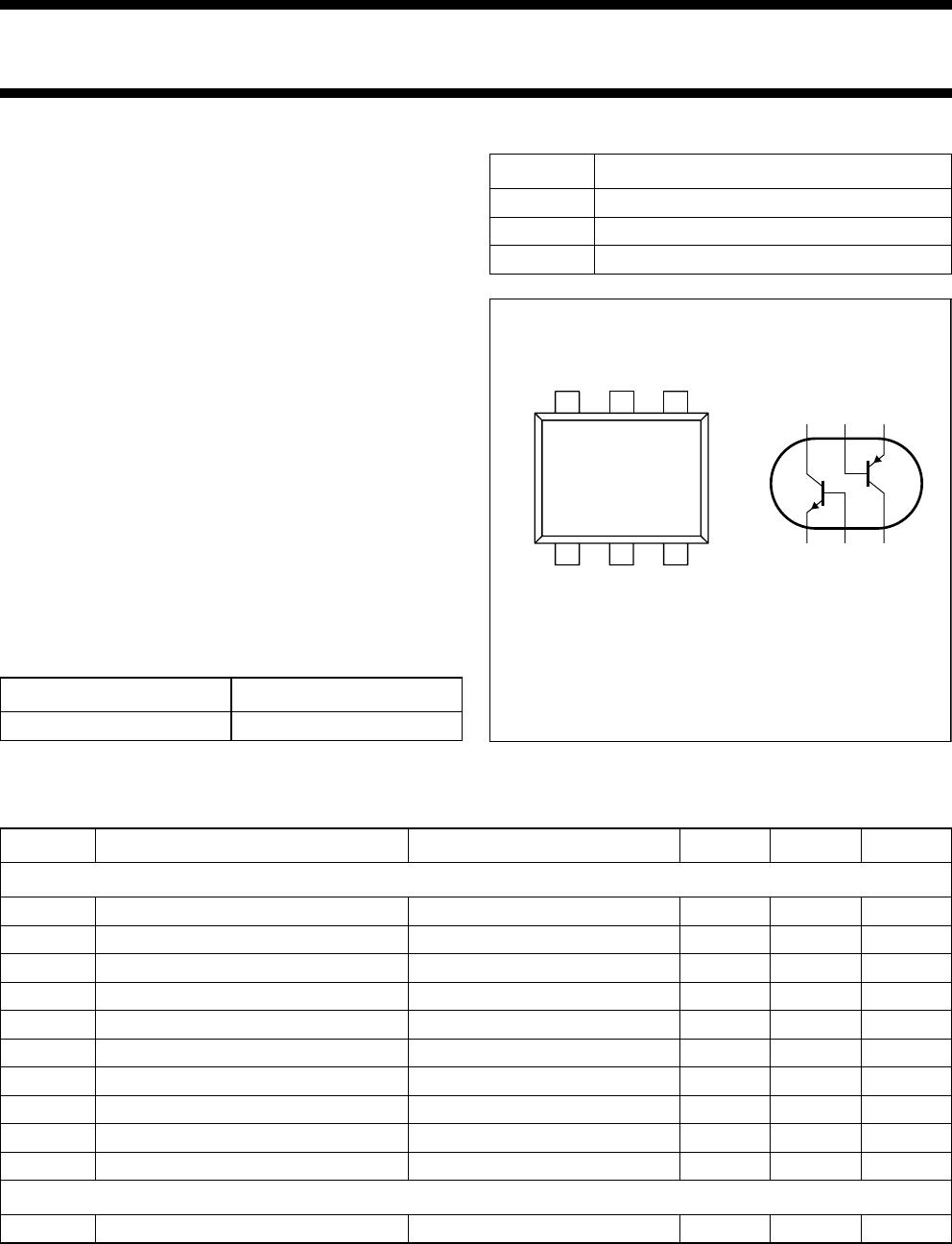
PINNING
TYPE NUMBER MARKING CODE
BC847BVN 13
PIN DESCRIPTION
1, 4 emitter TR1; TR2
2, 5 base TR1; TR2
6, 3 collector TR1; TR2
handbook, halfpage
MAM443
132
TR1
TR2
6
4
5
123
46
5
Top view
Fig.1 Simplified outline (SOT666) and symbol.
LIMITING VALUES
In accordance with the Absolute Maximum Rating System (IEC 60134).
Note
1. Transistor mounted on an FR4 printed-circuit board.
SYMBOL PARAMETER CONDITIONS MIN. MAX. UNIT
Per transistor; for the PNP transistor with negative polarity
V
CBO
collector-base voltage open emitter − 50 V
V
CEO
collector-emitter voltage open base − 45 V
V
EBO
emitter-base voltage open collector − 5 V
I
C
collector current (DC) − 100 mA
I
CM
peak collector current − 200 mA
I
BM
peak base current − 200 mA
P
tot
total power dissipation T
amb
≤ 25 °C; note 1 − 200 mW
T
stg
storage temperature −65 +150 °C
T
j
junction temperature − 150 °C
T
amb
operating ambient temperature −65 +150 °C
Per device
P
tot
total power dissipation T
amb
≤ 25 °C; note 1 − 300 mW