1
LTC1157
3.3V Dual Micropower
High-Side/Low-Side MOSFET Driver
The LTC1157 dual 3.3V micropower MOSFET gate driver
makes it possible to switch either supply or ground
reference loads through a low R
DS(ON)
N-channel switch
(N-channel switches are required at 3.3V because P-
channel MOSFETs do not have guaranteed R
DS(ON)
with
V
GS
≤ 3.3V). The LTC1157 internal charge pump boosts
the gate drive voltage 5.4V above the positive rail (8.7V
above ground), fully enhancing a logic level N-channel
switch for 3.3V high-side applications and a standard N-
channel switch for 3.3V low-side applications. The gate
drive voltage at 5V is typically 8.8V above supply (13.8V
above ground), so standard N-channel MOSFET switches
can be used for both high-side and low-side applications.
Micropower operation, with 3µA standby current and
80µA operating current, makes the LTC1157 well suited
for battery-powered applications.
The LTC1157 is available in both 8-pin DIP and SOIC.
S
F
EA
T
U
RE
■
Allows Lowest Drop 3.3V Supply Switching
■
Operates on 3.3V or 5V Nominal Supplies
■
3 Microamps Standby Current
■
80 Microamps ON Current
■
Drives Low Cost N-Channel Power MOSFETs
■
No External Charge Pump Components
■
Controlled Switching ON and OFF Times
■
Compatible with 3.3V and 5V Logic Families
■
Available in 8-Pin SOIC
U
S
A
O
PP
L
IC
AT
I
■
Notebook Computer Power Management
■
Palmtop Computer Power Management
■
P-Channel Switch Replacement
■
Battery Charging and Management
■
Mixed 5V and 3.3V Supply Switching
■
Stepper Motor and DC Motor Control
■
Cellular Telephones and Beepers
D
U
ESCRIPTIO
U
A
O
PP
L
IC
AT
ITY
P
I
CA
L
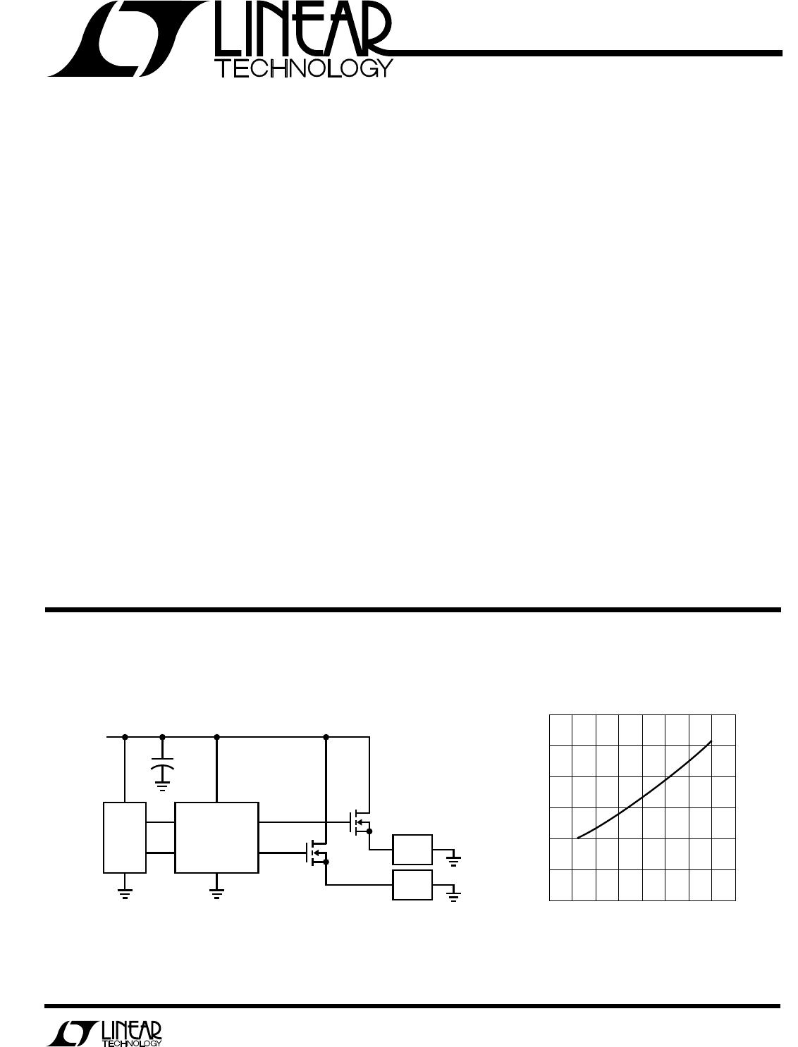
+
V
S
GND
G2
G1
IN2
IN1
LTC1157
3.3V
LOGIC
(8.7V)
(8.7V)
IRLR024
IRLR024
3.3V
LOAD
3.3V
LOAD
10µF
3.3V
LTC1157 • TA01
Ultra Low Voltage Drop 3.3V Dual High-Side Switch Gate Voltage Above Supply
SUPPLY VOLTAGE (V)
2.0
0
GATE VOLTAGE – SUPPLY VOLTAGE (V)
2
4
6
8
3.0 4.0
5.0
6.0
LTC1157 • TA02
10
12
2.5 3.5 4.5
5.5