LTC4440
10
4440fb
For more information www.linear.com/LTC4440
APPLICATIONS INFORMATION
Undervoltage Lockout (UVLO)
The LTC4440 contains both low side and high side un-
dervoltage lockout
detectors that monitor V
CC
and the
bootstrapped supply V
BOOST–TS
. When V
CC
falls below
6.2V, the internal buffer is disabled and the output pin
OUT is pulled down to TS. When V
BOOSTTS
falls below
6.9V, OUT is pulled down to TS. When both supplies are
undervoltage, OUT is pulled low to TS and the chip enters
a low current mode, drawing approximately 25µA from
V
CC
and 86µA from BOOST.
Bypassing and Grounding
The LTC4440 requires proper bypassing on the V
CC
and V
BOOST–TS
supplies due to its high speed switching
(nanoseconds) and large AC currents (Amperes). Careless
component placement and PCB trace routing may cause
excessive ringing and under/overshoot.
To obtain the optimum performance from the LTC4440:
A. Mount the bypass capacitors as close as possible
between the V
CC
and GND pins and the BOOST and
TS pins. The leads should be shortened as much as
possible to reduce lead inductance.
B. Use a low inductance, low impedance ground plane
to reduce any ground drop and stray capacitance. Re
-
member that
the LTC4440 switches >2A peak currents
and
any significant ground drop will degrade signal
integrity.
C. Plan the power/ground routing carefully. Know where
the large load switching current is coming from and
going to. Maintain separate ground return paths for
the input pin and the output power stage.
D. Keep the copper trace between the driver output pin
and the load short and wide.
E. When using the MS8E package, be sure to solder the
exposed pad on the back side of the LTC4440 package
to the board. Correctly soldered to a 2500mm
2
double-
sided 1oz copper board, the LTC4440 has a thermal
resistance of approximately 40°C/W. Failure to make
good thermal contact between the exposed back side
and the copper board will result in thermal resistances
far greater than 40°C/W.
LTC4440
11
4440fb
For more information www.linear.com/LTC4440
TYPICAL APPLICATIONS
18
10
911
12V
V
IN
12
LTC3722EGN-1
PDLY
OUTF
OUTE
COMPSSPGNDGND
CS
V
IN
SBUS
UVLO
1µF
ADLY
330pF
MMBT3904
2.2nF
100k
D12
5.1V
T3
1(1.5mH):0.5
T1
5(105µH):1:1
T2
5:5(105µH):1:1
2.49k
9.53k
10k
2.7k
470Ω
1/4W
L4
1mH
C3
68µF
20V
V
H
16
15
8
1 9
5
4
150Ω
0.02Ω
1.5W
30.1k
220pF
100Ω
330Ω
1.10k
909Ω
4.87k
1/4W
4.87k
1/4W
51Ω
2W
220pF
182k
20k
1/4W
220pF
4.99k
20k
180pF
68nF
220pF0.47µF
150k
SYNC PV
CC
CSE
+
LTC3901EGN
CSE
8
6 5
1
4 10 13 7
1µF
1µF
4440 TA03
–V
OUT
V
OUT
–V
OUT
D10
10V
V
OUT
ME ME2
GND PGND GND2 PGND2 TIMER
V
CC
330pF
2 3
1.10k 909Ω
39.2k
100Ω
1k
CSF
+
–V
OUT
V
OUT
V
OUT
–V
OUT
V
OUT
12V/35A
–V
OUT
CSF
11 12
MF MF2
14 15 16
22nF
Si7852DP
×4
Si7852DP
×4
Si7852DP
×2
L1
1.3µH
114
2
12V
D7
D8
4
2
1
6
10
8
7
+
1
0.22µF
Si7852DP
×2
3
6
7
824
A
D2
LTC4440EMS8E
BOOSTINP
TG
TSGNDGND
V
CC
12V
1
0.22µF
Si7852DP
×2
3
6
7
8
12VD
24
C
D3
D4
D5
51Ω
2W
0.47µF
100V
LTC4440EMS8E
BOOSTINP
TG
TSGNDGND
V
CC
12V
1µF
100V
×4
V
IN
V
IN
–V
IN
36V TO 72V
1µF
100V
17
D
OUTD
19
10Ω
10Ω
C
OUTC
20
B
OUTB
21
A
OUTA
C1, C2
180µF
16V
×2
+
1µF
0.47µF, 100V TDK C3216X7R2A474M
1µF, 100V TDK C4532X7R2A105M
C1,C2: SANYO 16SP180M
C3: AVX TPSE686M020R0150
C4: MURATA DE2E3KH222MB3B
D1, D4-D6: MURS120T3
D2, D3, D7, D8: BAS21
D9: MMBZ5226B
D10: MMBZ5240B
D11: BAT54
D12: MMBZ231B
L1: SUMIDA CDEP105-1R3MC-50
L2: PULSE PA0651
L3: PA1294.910
L4: COILCRAFT DO1608C-105
Q1, Q2: ZETEX FMMT619
Q3, Q4: ZETEX FMMT718
T1, T2: PULSE PA0526
T3: PULSE PA0785
6
3
422236
33k
5 7
D11
8.25k
I
SNS
5V
REF
I
SNS
0.1µF
5 8
1
2
1
MOC207
C4
2.2nF
250V
0.047µF
3
6
5
8
GND-F
V
+
GND-S
COLL REF
LT1431CS8
1.1k
22Ω
200k
750Ω
100Ω
D9 3.3V
0.02Ω
1.5W
V
H
D1
D6
13k
1/2W
0.47µF
100V
820pF
200V
L3
0.85µH
15Ω
1W
0.47µF
100V
Si7852DP
×2
12VB
Q1
Q3
Q2
Q4
11
10
8
7
MMBT3904
FBSPRG
R
LEB
10k
13
SYNC
5.1k
1
NC
8
DPRG
2
V
REF
5V
REF
14
C
T
24
L2
150nH
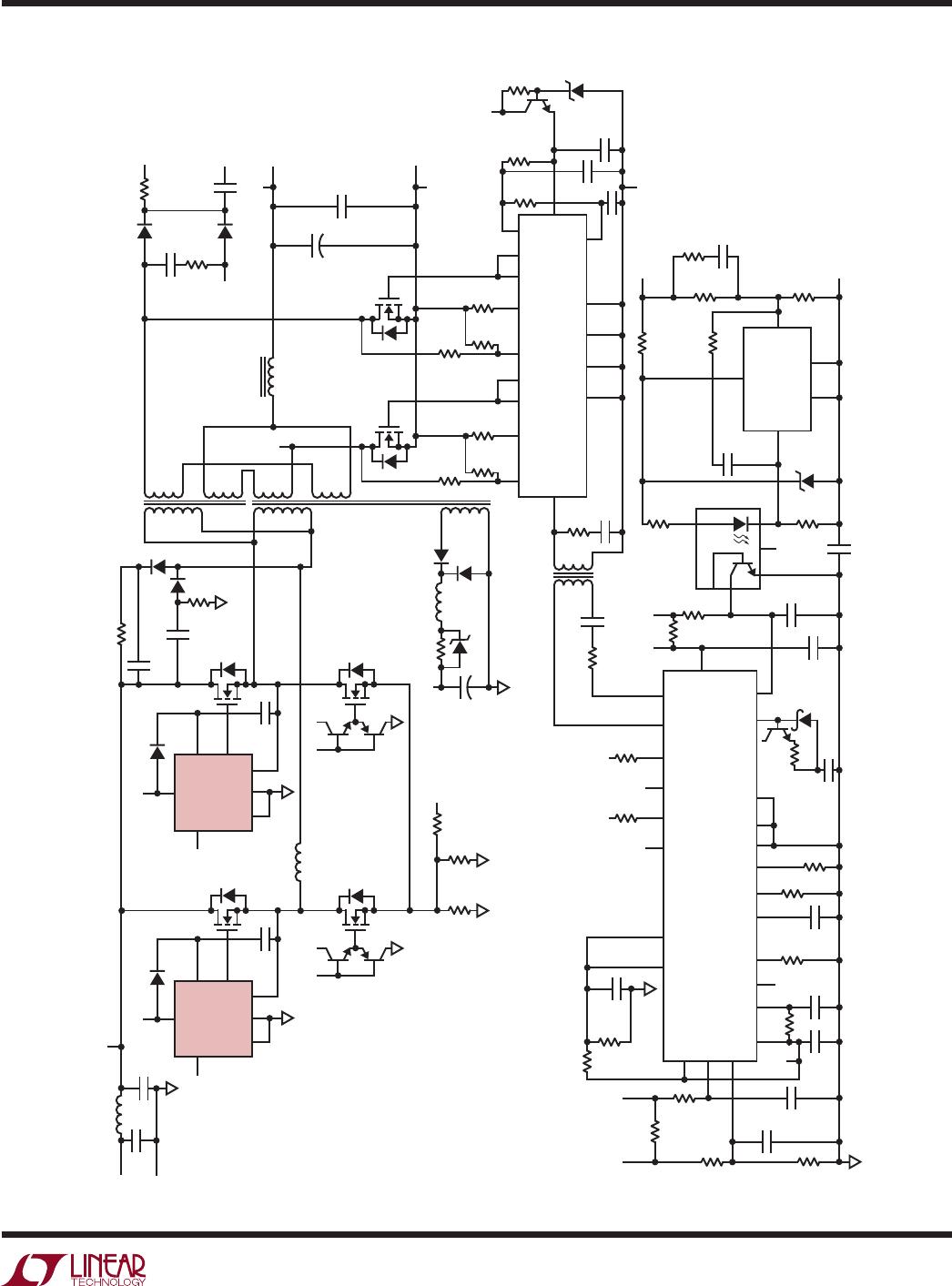
LTC3722/LTC4440 420W 36V-72V
IN
to 12V/35A Isolated Full-Bridge Supply
LTC4440
12
4440fb
For more information www.linear.com/LTC4440
TYPICAL APPLICATIONS
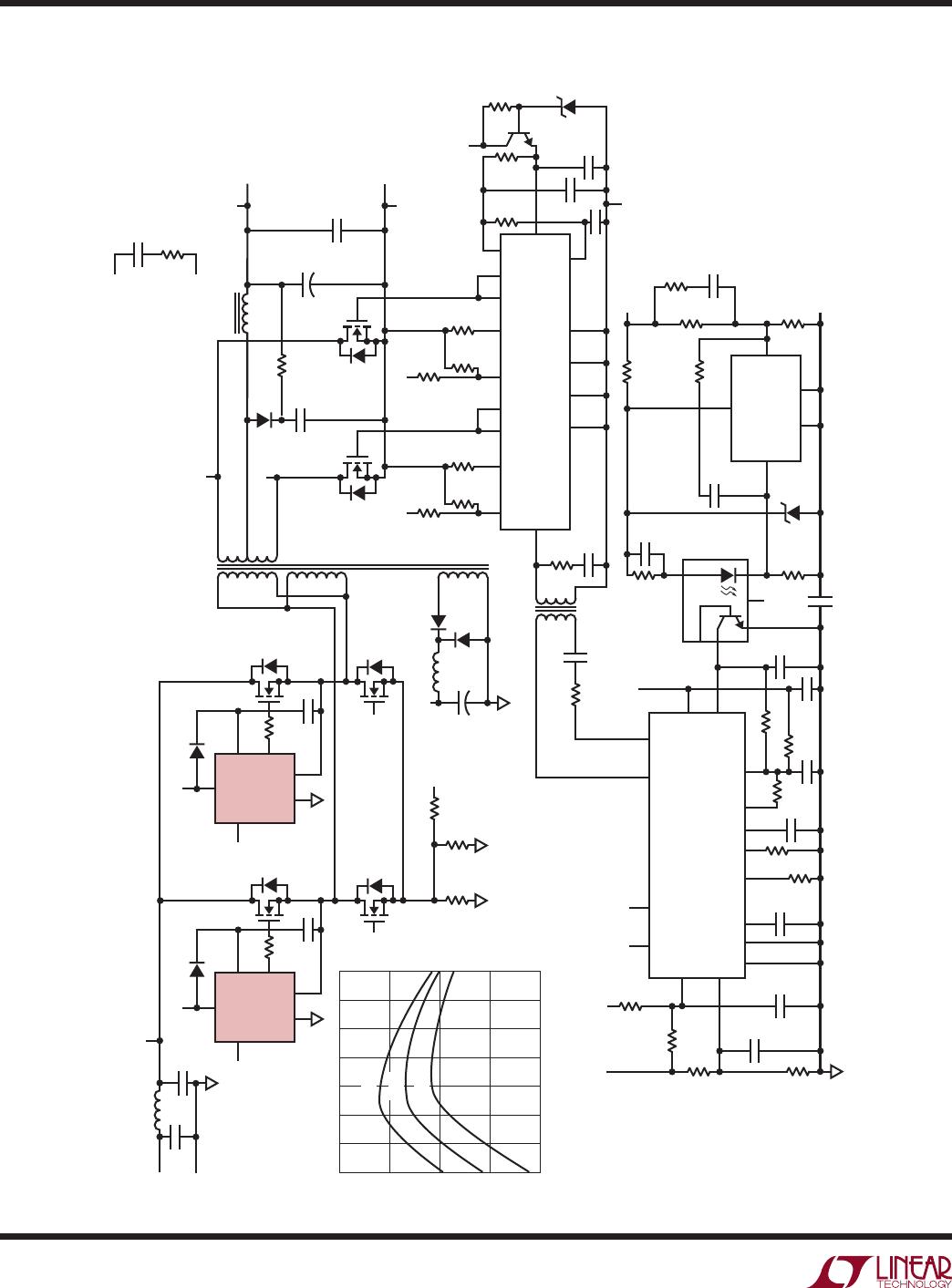
LTC3723-1 240W 42-56V
IN
to 12V/20A Isolated 1/4Brick (2.3" × 1.45")
5
46
A
B
12V
V
IN
15
LTC3723EGN-1
DRVB
SDRB
SDRA
COMP
CS
V
CC
UVLO
9
150k
1
0.47µF
1µF
DRVA
DPRG V
REF
SPRGGND SSFB C
T
330pF
22nF
100k
D8
10V
68nF
270pF
T2
1(1.5mH):0.5
T1
4T:6T(65µHMIN):6T:2T:2T
243k
2.49k
9.53k
10k
750Ω
1k
100Ω
1/4W
813
3
Si7370DP
×2
L4
1mH
C3
68µF
20V
V
F
D2
3
2
8
1 9
5
4
16
10k
33k
200Ω
1/4W
R1
0.03Ω
1.5W
66.5k
RLEB
127 14
220pF
22nF
100
665Ω
1k
866Ω
6.19k
1/4W
1.5nF
464k
30k
1/4W
SYNC PV
CC
CSF
+
V
F
LTC3901EGN
CSF
8
11 12
1
4 10 13 7
22nF
1µF
4.7µF
4440 TA05
–V
OUT
V
OUT
–V
OUT
D7
10V
V
OUT
MF MF2
GND PGND GND2 PGND2 TIMER
V
CC
470pF
14 15
1k 866Ω
42.2k
1k
100Ω
6.19k
1/4W
CSE
+
V
E
–V
OUT
V
OUT
V
F
V
OUT
12V/20A
–V
OUT
CSE
6 5
ME ME2
2 3 16
Si7370DP
×2
Si7852DPSi7852DP
L5
0.56µH
112
4
12V
D5
D6
3
5
1
6
9
7
V
E
+
0.1µF
Si7852DP
1
6
5
4
B
2
A
D3
LTC4440ES6
BOOSTINP
TG
TSGND
V
CC
12V
3
0.1µF
Si7852DP
1
6
5
42
B
D4
LTC4440ES6
BOOSTINP
TG
TSGND
V
CC
12V
1µF
100V
×3
V
IN
V
IN
–V
IN
42V TO 56V
1µF
100V
C1, C2
47µF
16V
×2
+
1µF
1µF
100V
1k
1/4W
1µF, 100V TDK C3225X7R2A105M
C1,C2: SANYO 16TQC47M
C3: AVX TPSE686M020R0150
C4: MURATA GHM3045X7R222K-GC
D2: DIODES INC. ES1B
D3-D6: BAS21
D7, D8: MMBZ5240B
L4: COILCRAFT DO1608C-105
L5: COILCRAFT DO1813P-561HC
L6: PULSE PA1294.132 OR
PANASONIC ETQP1H1R0BFA
R1, R2: IRC LRC2512-R03G
T1: PULSE PA0805.004
T2: PULSE PA0785
6
10
I
SNS
I
SNS
0.1µF
11
5 8
1
2
1
MOC207
C4
2.2nF
250V
0.1µF
3
6
5
8
GND-F
V
+
GND-S
COLL REF
LT1431CS8
A
1.5k
22Ω
4.7Ω4.7Ω
R2
0.03Ω
1.5W
V
E
470pF
100V
L6
1.25µH
10Ω
1W
6
93
EFFICIENCY (%)
94
95
96
97
8 10 12
LOAD CURRENT (A)
14
16 18 20
42V
IN
48V
IN
56V
IN
MMBT3904

LTC4440IMS8E#TRPBF

Mfr. #:
Manufacturer:
Analog Devices / Linear Technology
Description:
Gate Drivers High & Low-Side Driver
Lifecycle:
New from this manufacturer.
Delivery:
DHL FedEx Ups TNT EMS
Payment:
T/T Paypal Visa MoneyGram Western Union