LTC4440
4
4440fb
For more information www.linear.com/LTC4440
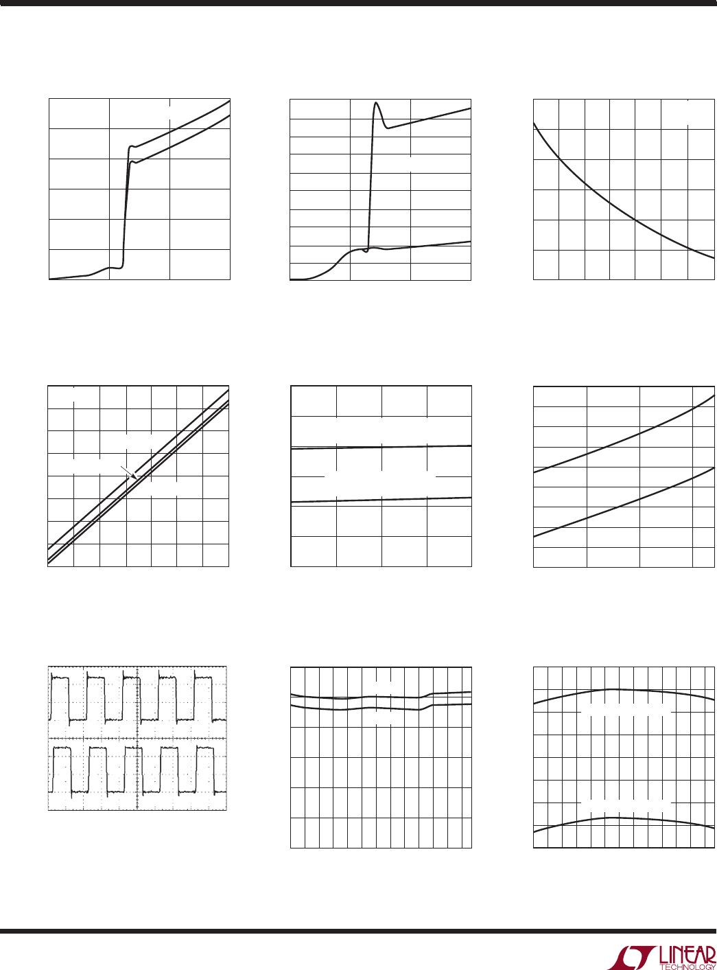
TYPICAL PERFORMANCE CHARACTERISTICS
V
CC
Supply Quiescent Current
vs Voltage
BOOST – TS
Supply Quiescent
Current vs Voltage
Output Low Voltage (V
OL
)
vs Supply Voltage
V
CC
SUPPLY VOLTAGE (V)
0
0
QUIESCENT CURRENT (µA)
50
100
150
200
300
5 10
4440 G01
15
250
INP = V
CC
INP = 0V
T
A
= 25°C
BOOST – TS SUPPLY VOLTAGE (V)
0
0
QUIESCENT CURRENT (µA)
100
150
200
250
300
350
5
10
4440 G02
400
450
INP = 0V
500
50
15
INP = V
CC
T
A
= 25°C
BOOST – TS SUPPLY VOLTAGE (V)
8
OUTPUT (TG – TS) VOLTAGE (mV)
150
155
160
165
170
11 13
4440 G03
145
140
9 10
12 14 15
I
TG
= 100mA
T
A
= 25°C
2MHz Operation
V
CC
Supply Current (V
CC
= 12V)
vs Temperature
V
CC
Undervoltage Lockout
Thresholds vs Temperature
Output High Voltage (V
OH
)
vs Supply Voltage
Input Thresholds (INP)
vs Supply Voltage
V
CC
Supply Current
at TTL Input Levels
BOOST – TS SUPPLY VOLTAGE (V)
8
OUTPUT VOLTAGE (TG –TS) (V)
14
11
4440 G04
11
9
9 10 12
8
7
15
13
12
10
13 14
15
I
TG
= –100mA
I
TG
= –1mA
I
TG
= –10mA
T
A
= 25°C
V
CC
SUPPLY VOLTAGE (V)
7
0.8
1.0
1.2
1.4
1.6
1.8
9 11 13
V
IL
(INPUT LOW THRESHOLD)
V
IH
(INPUT HIGH THRESHOLD)
T
A
= 25°C
TEMPERATURE (°C)
60
CURRENT (µA)
200
250
300
12090
4440 G08
150
100
0
–30
300 60
50
INP = 0V
INP = 12V
V
CC
SUPPLY VOLTAGE (V)
8
V
CC
SUPPLY QUIESCENT CURRENT (µA)
300
320
340
4440 G06
280
260
200
10
12
14
240
220
380
INP = 2V
INP = 0.8V
360
T
A
= 25°C
TEMPERATURE (°C)
60
V
CC
SUPPLY VOLTAGE (V)
6.45
6.40
6.55
6.50
6.35
6.30
6.25
6.20
6.15
12090
4440 G09
–30
300 60
FALLING THRESHOLD
RISING THRESHOLD
250ns/DIVV
CC
= 12V
INPUT
(INP)
5V/DIV
OUTPUT
(TG)
5V/DIV
4440 G07
LTC4440
5
4440fb
For more information www.linear.com/LTC4440
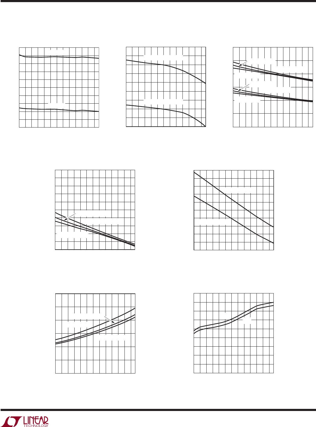
Boost Supply Current
vs Temperature
Boost Supply (BOOST – TS)
Undervoltage Lockout Thresholds
vs Temperature
Input Threshold vs Temperature
TEMPERATURE (°C)
60
CURRENT (µA)
500
400
450
350
300
250
200
150
100
50
12090
4440 G10
0
–30
300 60
INP = 0V
INP = 12V
TEMPERATURE (°C)
60
BOOST – TS SUPPLY VOLTAGE (V)
7.6
7.5
7.4
7.3
7.2
7.1
7.0
6.9
6.8
12090
4440 G11
6.7
–30
300 60
FALLING THRESHOLD
RISING THRESHOLD
TEMPERATURE (°C)
60
INPUT THRESHOLD (V)
1.6
1.8
2.0
12090
4440 G12
1.4
1.2
0.8
–30
300 60
1.0
V
IH
(V
CC
= 15V)
V
IL
(V
CC
= 15V)
V
IH
(V
CC
= 8V)
V
IL
(V
CC
= 8V)
V
IH
(V
CC
= 12V)
V
IL
(V
CC
= 12V)
TYPICAL PERFORMANCE CHARACTERISTICS
Output Driver Pull-Down
Resistance vs Temperature
Propagation Delay vs Temperature
(V
CC
= BOOST = 12V)
Input Threshold Hysteresis
vs Temperature
Peak Driver (TG) Pull-Up Current
vs Temperature
TEMPERATURE (°C)
60
HYSTERESIS (mV)
500
460
480
440
420
400
380
360
340
320
12090
4440 G13
300
–30
300 60
V
IH
-V
IL
(V
CC
= 12V)
V
IH
-V
IL
(V
CC
= 15V)
V
IH
-V
IL
(V
CC
= 8V)
TEMPERATURE (°C)
60
PEAK CURRENT (A)
3.0
2.8
2.9
2.7
2.6
2.5
2.4
2.3
2.2
2.1
12090
4440 G14
2.0
–30
300 60
BOOST – TS = 12V
BOOST – TS = 15V
TEMPERATURE (°C)
60
R
DS
(Ω)
2.0
2.5
3.0
12090
4440 G15
1.5
1.0
0
–30
300 60
0.5
BOOST – TS = 15V
BOOST – TS = 8V
BOOST – TS = 12V
TEMPERATURE (°C)
60
PROPAGATION DELAY (ns)
45
40
35
30
25
20
15
10
5
12090
4440 G16
0
–30
300 60
t
PLH
t
PHL
LTC4440
6
4440fb
For more information www.linear.com/LTC4440
PIN FUNCTIONS
V
CC
(Pin 1): Chip Supply. This pin powers the internal
low side circuitry. A low ESR ceramic bypass capacitor
should be tied between this pin and the GND pin (Pin 2).
GND (Pin 2): Chip Ground.
INP (Pin 3): Input Signal. TTL/CMOS compatible input
referenced to GND (Pin 2).
TS (Pin 4): Top (High Side) Source Connection.
TG (Pin 5): High Current Gate Driver Output (Top Gate).
This pin swings between TS and BOOST.
BOOST (Pin 6): High Side Bootstrapped Supply. An
external capacitor should be tied between this pin and
TS (Pin 4). Normally, a bootstrap diode is connected
between V
CC
(Pin1) and this pin. Voltage swing at this
pin is from V
CC
V
D
to V
IN
+ V
CC
V
D
, where V
D
is the
forward voltage drop of the bootstrap diode.
SOT-23 Package
INP (Pin 1): Input Signal. TTL/CMOS compatible input
referenced to GND (Pin 2).
GND (Pins 2, 4): Chip Ground.
V
CC
(Pin 3): Chip Supply. This pin powers the internal
low side circuitry. A low ESR ceramic bypass capacitor
should be tied between this pin and the GND pin (Pin 2).
NC (Pin 5): No Connect. No connection required. For
convenience, this pin may be tied to Pin 6 (BOOST) on
the application board
.
BO
OST (Pin 6): High Side Bootstrapped Supply. An external
capacitor should be tied between this pin and TS (Pin8).
Normally, a bootstrap diode is connected between V
CC
(Pin3) and this pin. Voltage swing at this pin is from V
CC
V
D
to V
IN
+ V
CC
V
D
, where V
D
is the forward voltage
drop of the bootstrap diode.
TG (Pin 7): High Current Gate Driver Output (Top Gate).
This pin swings between TS and BOOST.
TS (Pin 8): Top (High Side) Source Connection.
Exposed Pad (Pin 9): Ground. Must be electrically con
-
nected to Pins 2 and 4 and soldered to PCB ground for
optimum thermal performance.
Exposed Pad MS8E Package
LTC4440IMS8E#TRPBF

Mfr. #:
Manufacturer:
Analog Devices / Linear Technology
Description:
Gate Drivers High & Low-Side Driver
Lifecycle:
New from this manufacturer.
Delivery:
DHL FedEx Ups TNT EMS
Payment:
T/T Paypal Visa MoneyGram Western Union