SA5.0A thru SA170CA
www.vishay.com
Vishay General Semiconductor
Revision: 23-Jan-14
2
Document Number: 88378
For technical questions within your region: DiodesAmericas@vishay.com
, DiodesAsia@vishay.com, DiodesEurope@vishay.com
THIS DOCUMENT IS SUBJECT TO CHANGE WITHOUT NOTICE. THE PRODUCTS DESCRIBED HEREIN AND THIS DOCUMENT
ARE SUBJECT TO SPECIFIC DISCLAIMERS, SET FORTH AT www.vishay.com/doc?91000
Notes
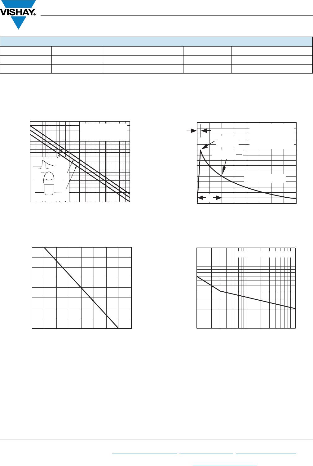
(1)
Pulse test: t
p
50 ms
(2)
Surge current waveform per fig. 3 and derate per fig. 2
(3)
For bi-directional types with V
WM
of 10 V and less the I
D
limit is doubled
(4)
For the bi-directional SA5.0CA, the maximum V
BR
is 7.25 V
(5)
All terms and symbols are consistent with ANSI/EEE CA62.35
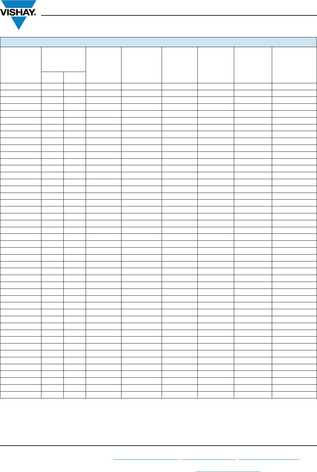
ELECTRICAL CHARACTERISTICS (T
A
= 25 °C unless otherwise noted)
DEVICE TYPE
BREAKDOWN
VOLTAGE
V
BR
AT I
T
(1)
(V)
TEST
CURRENT
I
T
(mA)
STAND-OFF
VOLTAGE
V
WM
(V)
MAXIMUM
REVERSE
LEAKAGE
AT V
WM
(3)
I
D
(μA)
MAXIMUM
PEAK
PULSE
CURRENT
I
PPM
(2)
(A)
MAXIMUM
CLAMPING
VOLTAGE
AT I
PPM
V
C
(V)
MAXIMUM
TEMPERATURE
COEFFICENT
AT V
BR
(mV/°C)
MIN. MAX.
SA5.0A
(4)
6.40 7.07 10 5.0 600 54.3 9.2 5
SA6.0A 6.67 7.37 10 6.0 600 48.5 10.3 5
SA6.5A 7.22 7.98 10 6.5 400 44.7 11.2 5
SA7.0A 7.78 8.60 10 7.0 150 41.7 12.0 6
SA7.5A 8.33 9.21 1.0 7.5 50 38.8 12.9 7
SA8.0A 8.89 9.83 1.0 8.0 25 36.8 13.6 7
SA8.5A 9.44 10.4 1.0 8.5 10 34.7 14.4 8
SA9.0A 10.0 11.1 1.0 9.0 5.0 32.5 15.4 9
SA10A 11.1 12.3 1.0 10 1.0 29.4 17.0 10
SA11A 12.2 13.5 1.0 11 1.0 27.5 18.2 11
SA12A 13.3 14.7 1.0 12 1.0 25.1 19.9 12
SA13A 14.4 15.9 1.0 13 1.0 23.3 21.5 13
SA14A 15.6 17.2 1.0 14 1.0 21.6 23.2 14
SA15A 16.7 18.5 1.0 15 1.0 20.5 24.4 16
SA16A 17.8 19.7 1.0 16 1.0 19.2 26.0 17
SA17A 18.9 20.9 1.0 17 1.0 18.1 27.6 19
SA18A 20.0 22.1 1.0 18 1.0 17.1 29.2 20
SA20A 22.2 24.5 1.0 20 1.0 15.4 32.4 23
SA22A 24.4 26.9 1.0 22 1.0 14.1 35.5 25
SA24A 26.7 29.5 1.0 24 1.0 12.9 38.9 28
SA26A 28.9 31.9 1.0 26 1.0 11.9 42.1 30
SA28A 31.1 34.4 1.0 28 1.0 11 45.4 31
SA30A 33.3 36.8 1.0 30 1.0 10 48.4 36
SA33A 36.7 40.6 1.0 33 1.0 9.4 53.3 39
SA36A 40.0 44.2 1.0 36 1.0 8.6 58.1 41
SA40A 44.4 49.1 1.0 40 1.0 7.8 64.5 46
SA43A 47.8 52.8 1.0 43 1.0 7.2 69.4 50
SA45A 50.0 55.3 1.0 45 1.0 6.9 72.7 52
SA48A 53.3 58.9 1.0 48 1.0 6.5 77.4 56
SA51A 56.7 62.7 1.0 51 1.0 6.1 82.4 61
SA54A 60.0 66.3 1.0 54 1.0 5.7 87.1 65
SA58A 64.4 71.2 1.0 58 1.0 5.3 93.6 70
SA60A 66.7 73.7 1.0 60 1.0 5.2 96.8 71
SA64A 71.1 78.6 1.0 64 1.0 4.9 103 76
SA70A 77.8 86.0 1.0 70 1.0 4.4 113 85
SA75A 83.3 92.1 1.0 75 1.0 4.1 121 91
SA78A 86.7 95.8 1.0 78 1.0 4 126 95
SA85A 94.4 104 1.0 85 1.0 3.6 137 103
SA90A 100 111 1.0 90 1.0 3.4 146 110
SA100A 111 123 1.0 100 1.0 3.1 162 123
SA110A 122 135 1.0 110 1.0 2.8 177 133
SA120A 133 147 1.0 120 1.0 2.6 193 146
SA130A 144 159 1.0 130 1.0 2.4 209 158
SA150A 167 185 1.0 150 1.0 2.1 243 184
SA160A 178 197 1.0 160 1.0 1.9 259 196
SA170A 189 209 1.0 170 1.0 1.8 275 208