© Semiconductor Components Industries, LLC, 1997
October, 2016 − Rev. 15
1 Publication Order Number:
BC817−16LT1/D
BC817-16L, SBC817-16L,
BC817-25L, SBC817-25L,
BC817-40L, SBC817-40L
General Purpose
Transistors
NPN Silicon
Features
• S and NSV Prefixes for Automotive and Other Applications
Requiring Unique Site and Control Change Requirements;
AEC−Q101 Qualified and PPAP Capable
• These Devices are Pb−Free, Halogen Free/BFR Free and are RoHS
Compliant
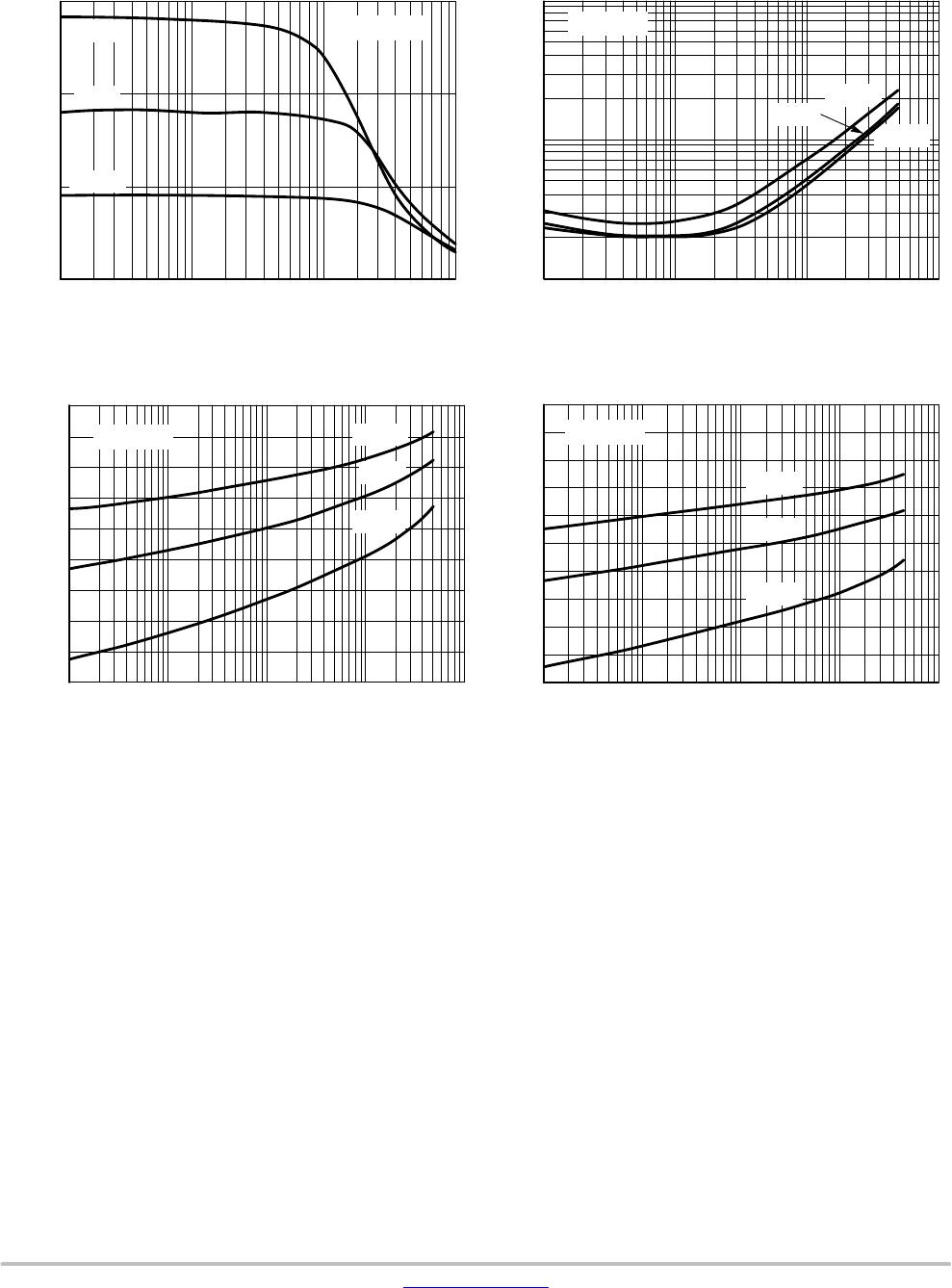
MAXIMUM RATINGS
Rating Symbol Value Unit
Collector − Emitter Voltage V
CEO
45 V
Collector − Base Voltage V
CBO
50 V
Emitter − Base Voltage V
EBO
5.0 V
Collector Current − Continuous I
C
500 mAdc
THERMAL CHARACTERISTICS
Characteristic Symbol Max Unit
Total Device Dissipation FR−5 Board,
(Note 1) T
A
= 25°C
Derate above 25°C
P
D
225
1.8
mW
mW/°C
Thermal Resistance,
Junction−to−Ambient
R
q
JA
556 °C/W
Total Device Dissipation
Alumina Substrate, (Note 2)
T
A
= 25°C
Derate above 25°C
P
D
300
2.4
mW
mW/°C
Thermal Resistance,
Junction−to−Ambient
R
q
JA
417 °C/W
Junction and Storage Temperature T
J
, T
stg
−65 to +150 °C
Stresses exceeding those listed in the Maximum Ratings table may damage the
device. If any of these limits are exceeded, device functionality should not be
assumed, damage may occur and reliability may be affected.
1. FR−5 = 1.0 x 0.75 x 0.062 in.
2. Alumina = 0.4 x 0.3 x 0.024 in 99.5% alumina.
See detailed ordering and shipping information in the package
dimensions section on page 2 of this data sheet.
ORDERING INFORMATION
COLLECTOR
3
1
BASE
2
EMITTER
SOT−23
CASE 318
STYLE 6
1
2
3
1
6x M G
G
6x = Device Code
x = A, B, or C
M = Date Code*
G = Pb−Free Package
MARKING DIAGRAM
(Note: Microdot may be in either location)
*Date Code orientation and/or overbar may
vary depending upon manufacturing location.
www.onsemi.com