1/8
www.rohm.com
2012.02 - Rev.
© 2012 ROHM Co., Ltd. All rights reserved.
Stepping Motor Driver series
Micro step 36V
Stepping Motor Drivers
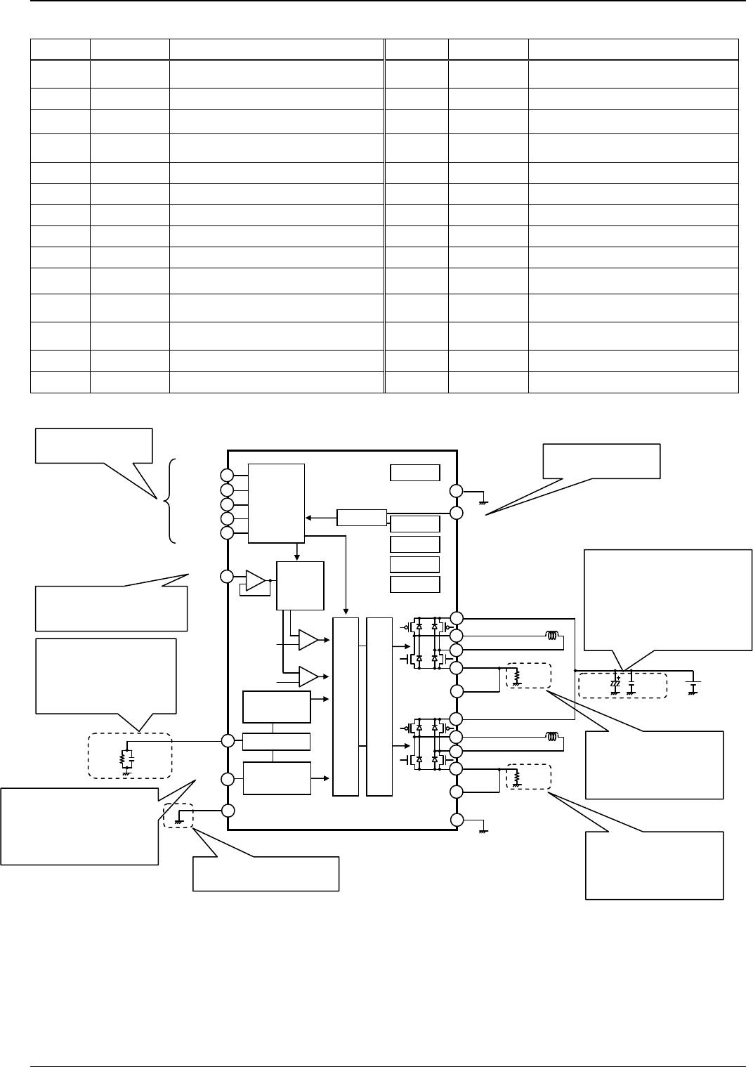
BD63843EFV, BD63847EFV
●Description
BD63843EFV / BD63847EFV are stepping motor drivers of 1/16 micro step(sixteenth step) drive. As for its basic function, it
is a low power consumption bipolar PWM constant current-drive driver with power supply rated voltage of 36V and rated
output current (DC) of 1.0A, 2.0A. The input interface is CLK-IN type.
There are step modes of Full step & Half step, Eighth step, Sixteenth step mode by internal DAC (D-A converter), and for
current decay mode, the ratio of FAST DECAY & SLOW DECAY can be freely set, so the optimum control conditions for
every motor can be realized. In addition, being able to drive with one system of power supply makes contribution to the set
design’s getting easy.
●Feature
1) Single power supply input (rated voltage of 36V)
2) Rated output current:(DC) 1.0A, 2.0A
3) Low ON resistance DMOS output
4) CLK-IN drive mode
5) PWM constant current control (other oscillation)
6) Built-in spike noise cancel function (external noise filter is unnecessary)
7) Full step, Half step, Eighth step, Sixteenth step drive
8) Timing free for changing step modes
9) Current decay mode switching function (linearly variable FAST/SLOW DECAY ratio)
10) Normal rotation & reverse rotation switching function
11) Power save function
12) Built-in logic input pull-down resistor
13) Power-on reset function
14) Thermal shutdown circuit (TSD)
15) Over current protection circuit (OCP)
16) Under voltage lock out circuit (UVLO)
17) Over voltage lock out circuit (OVLO)
18) Ghost Supply Prevention (protects against malfunction when power supply is disconnected)
19) Electrostatic discharge: 8kV (HBM specification)
20) Adjacent pins short protection
21) Inverted mounting protection
22) Microminiature, ultra-thin and high heat-radiation (exposed metal type) HTSSOP-B28 package
23) Pin-compatible line-up (In addition, pin-compatible to BD6387□EFV series)
●Application
PPC, multi-function printer, laser beam printer, ink jet printer, monitoring camera, WEB camera, sewing machine, photo
printer, FAX, scanner, mini printer, toy, and robot etc.
No.12009EAT08