4
COMMERCIAL AND INDUSTRIAL
TEMPERATURE RANGES
IDT72V01/72V02/72V03/72V04/72V05/72V06 3.3V ASYNCHRONOUS FIFO
512 x 9, 1,024 x 9, 2,048 x 9, 4,096 x 9, 8,192 x 9 and 16,384 x 9
SIGNAL DESCRIPTIONS
INPUTS:
DATA IN (D0 – D8)
Data inputs for 9-bit wide data.
CONTROLS:
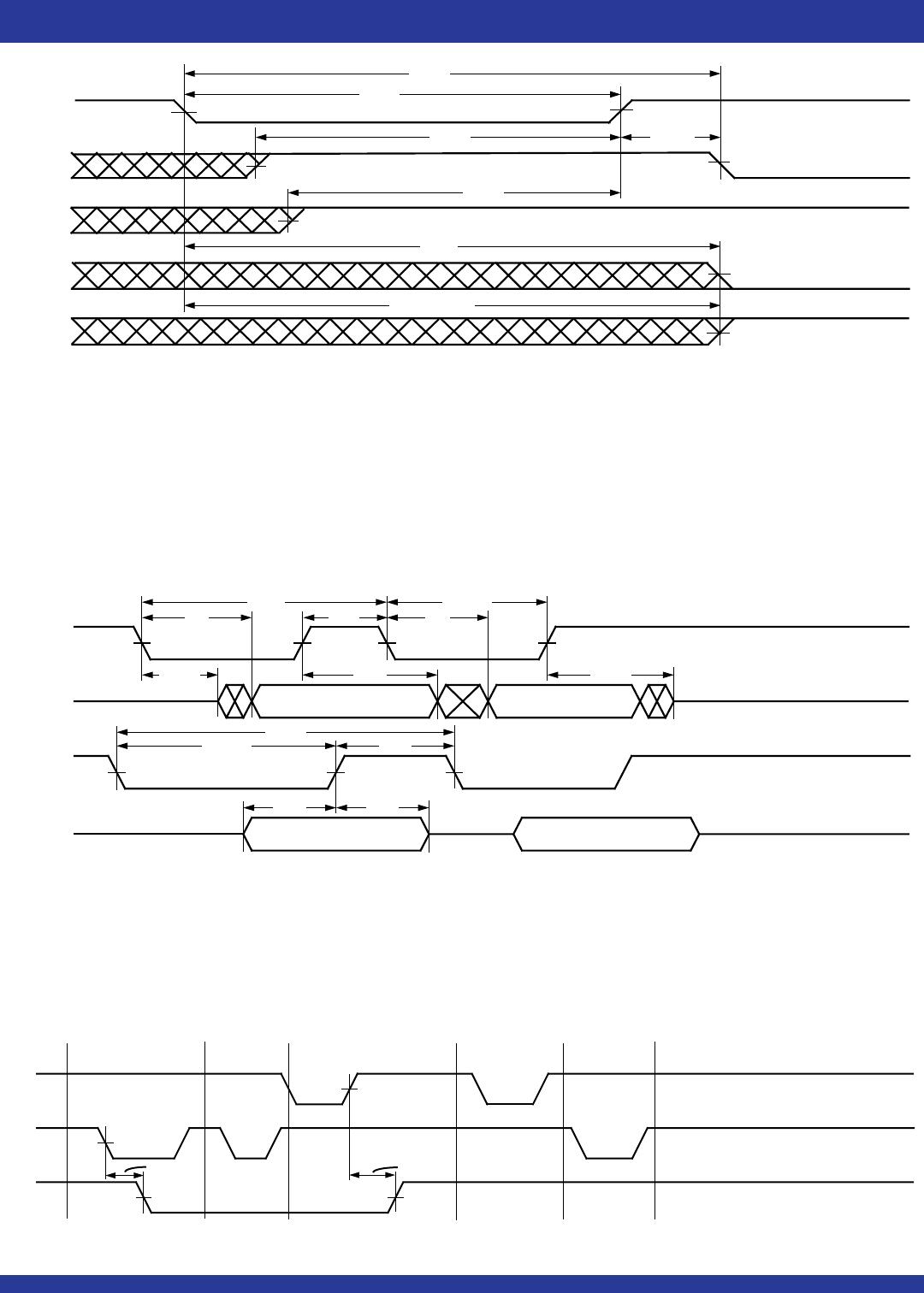
RESET (RS)
Reset is accomplished whenever the Reset (RS) input is taken to a LOW
state. During reset, both internal read and write pointers are set to the first
location. A reset is required after power up before a write operation can take
place. Both the Read Enable (R) and Write Enable (W) inputs must be
in the HIGH state during the window shown in Figure 2, (i.e., tRSS
before the rising edge of RS ) and should not change until tRSR after
the rising edge of RS. Half-Full Flag (HF) will be reset to HIGH after
Reset (RS).
WRITE ENABLE (W)
A write cycle is initiated on the falling edge of this input if the Full Flag (FF)
is not set. Data setup and hold times must be adhered to with respect to the rising
edge of the Write Enable (W). Data is stored in the RAM array sequentially and
independently of any ongoing read operation.
After half of the memory is filled and at the falling edge of the next write
operation, the Half-Full Flag (HF) will be set to LOW and will remain set until the
difference between the write pointer and read pointer is less than or equal to
one half of the total memory of the device. The Half-Full Flag (HF) is then reset
by the rising edge of the read operation.
To prevent data overflow, the Full Flag (FF) will go LOW, inhibiting further
write operations. Upon the completion of a valid read operation, the Full Flag
(FF) will go HIGH after tRFF, allowing a valid write to begin. When the FIFO
is full, the internal write pointer is blocked from W, so external changes in W will
not affect the FIFO when it is full.
READ ENABLE (R)
A read cycle is initiated on the falling edge of the Read Enable (R) provided
the Empty Flag (EF) is not set. The data is accessed on a First-In/First-Out basis,
independent of any ongoing write operations. After Read Enable (R) goes
HIGH, the Data Outputs (Q0 – Q8) will return to a high impedance condition until
the next Read operation. When all data has been read from the FIFO, the Empty
Flag (EF) will go LOW, allowing the “final” read cycle but inhibiting further read
operations with the data outputs remaining in a high impedance state. Once a
valid write operation has been accomplished, the Empty Flag (EF) will go HIGH
after tWEF and a valid Read can then begin. When the FIFO is empty, the internal
read pointer is blocked from R so external changes in R will not affect the FIFO
when it is empty.
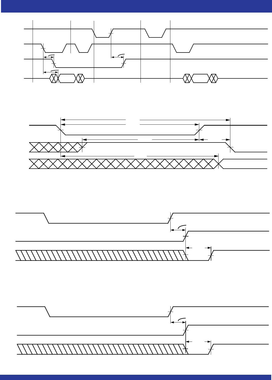
FIRST LOAD/RETRANSMIT (FL/RT)
This is a dual-purpose input. In the Depth Expansion Mode, this pin is
grounded to indicate that it is the first loaded (see Operating Modes). In the Single
Device Mode, this pin acts as the retransmit input. The Single Device Mode is
initiated by grounding the Expansion In (XI).
These FIFOs can be made to retransmit data when the Retransmit Enable
control (RT) input is pulsed LOW. A retransmit operation will set the internal read
pointer to the first location and will not affect the write pointer. Read Enable (R)
and Write Enable (W) must be in the HIGH state during retransmit. This feature
is useful when less than 512/1,024/2,048/4,096/8,192/16,384 writes are
performed between resets. The retransmit feature is not compatible with the
Depth Expansion Mode and will affect the Half-Full Flag (HF), depending on
the relative locations of the read and write pointers.
EXPANSION IN (XI)
This input is a dual-purpose pin. Expansion In (XI) is grounded to indicate
an operation in the single device mode. Expansion In (XI) is connected to
Expansion Out (XO) of the previous device in the Depth Expansion or Daisy
Chain Mode.
OUTPUTS:
FULL FLAG (FF)
The Full Flag (FF) will go LOW, inhibiting further write operation, when the
write pointer is one location less than the read pointer, indicating that the device
is full. If the read pointer is not moved after Reset (RS), the Full-Flag (FF) will
go LOW after 512/1,024/2,048/4,096/8,192/16,384 writes to the IDT72V01/
72V02/72V03/72V04/72V05/72V06.
EMPTY FLAG (EF)
The Empty Flag (EF) will go LOW, inhibiting further read operations, when
the read pointer is equal to the write pointer, indicating that the device is empty.
EXPANSION OUT/HALF-FULL FLAG (XO/HF)
This is a dual-purpose output. In the single device mode, when Expansion
In (XI) is grounded, this output acts as an indication of a half-full memory.
After half of the memory is filled and at the falling edge of the next write
operation, the Half-Full Flag (HF) will be set LOW and will remain set until the
difference between the write pointer and read pointer is less than or equal to
one half of the total memory of the device. The Half-Full Flag (HF) is then reset
by using rising edge of the read operation.
In the Depth Expansion Mode, Expansion In (XI) is connected to Expansion
Out (XO) of the previous device. This output acts as a signal to the next device
in the Daisy Chain by providing a pulse to the next device when the previous
device reaches the last location of memory.
DATA OUTPUTS (Q0 – Q8)
Data outputs for 9-bit wide data. This data is in a high impedance condition
whenever Read (R) is in a HIGH state.