TC4423/TC4424/TC4425
DS21421E-page 4 2002-2012 Microchip Technology Inc.
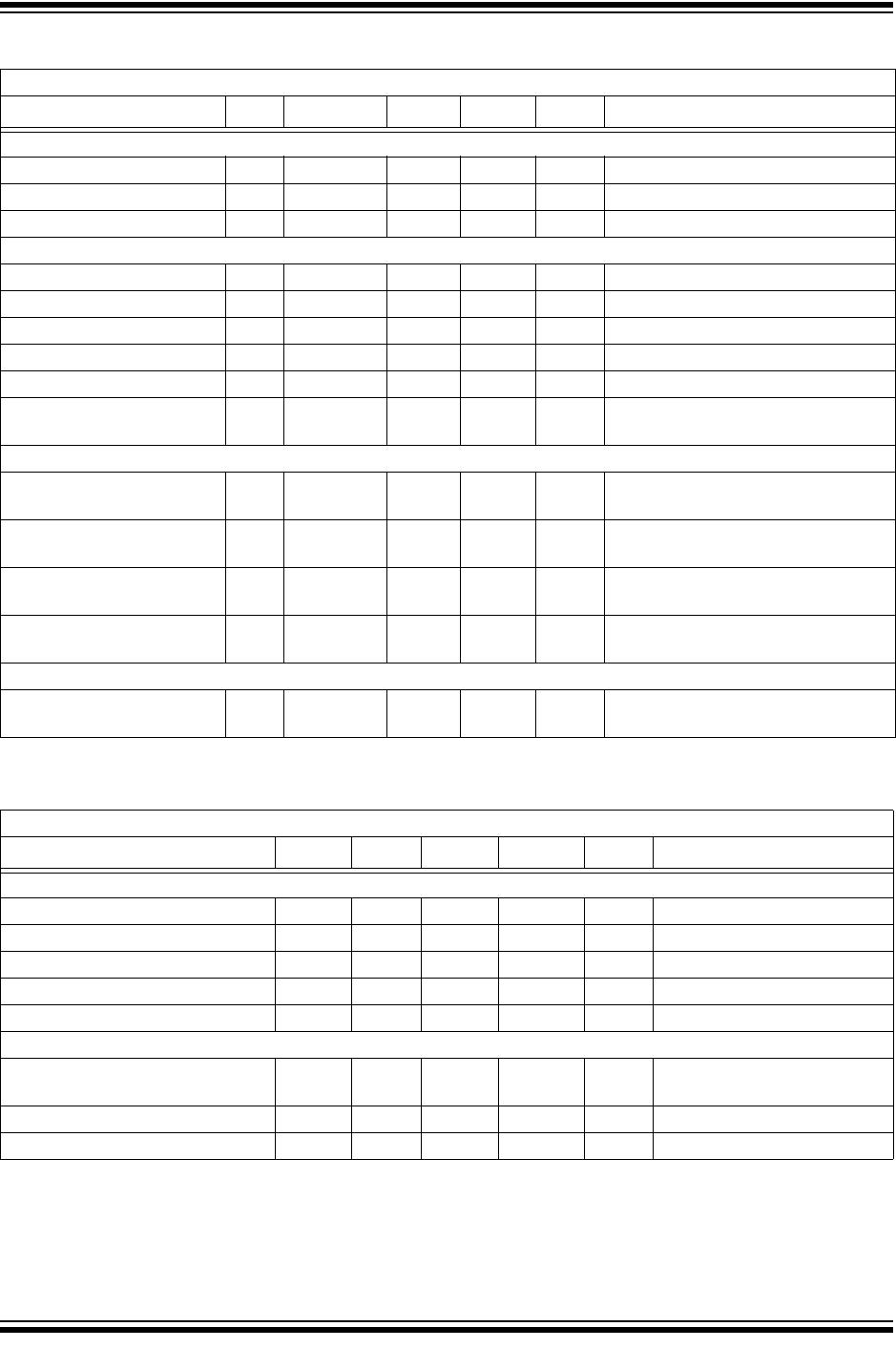
DC CHARACTERISTICS (OVER OPERATING TEMPERATURE RANGE)
TEMPERATURE CHARACTERISTICS
Electrical Specifications: Unless otherwise indicated, operating temperature range with 4.5V V
DD
18V.
Parameters Sym Min Typ Max Units Conditions
Input
Logic ‘1’, High Input Voltage V
IH
2.4 V
Logic ‘0’, Low Input Voltage V
IL
——0.8V
Input Current I
IN
–10 +10 µA 0VV
IN
V
DD
Output
High Output Voltage V
OH
V
DD
– 0.025 V
Low Output Voltage V
OL
——0.025V
Output Resistance, High R
OH
—3.78 I
OUT
= 10 mA, V
DD
= 18V
Output Resistance, Low R
OL
—4.38 I
OUT
= 10 mA, V
DD
= 18V
Peak Output Current I
PK
—3.0A
Latch-Up Protection
Withstand Reverse Current
I
REV
>1.5 A Duty cycle2%, t 300 µsec
Switching Time (Note 1)
Rise Time t
R
—2860nsFigure 4-1, Figure 4-2,
C
L
= 1800 pF
Fall Time t
F
—3260nsFigure 4-1, Figure 4-2,
C
L
= 1800 pF
Delay Time t
D1
32 100 ns Figure 4-1, Figure 4-2,
C
L
= 1800 pF
Delay Time t
D2
38 100 ns Figure 4-1, Figure 4-2,
C
L
= 1800 pF
Power Supply
Power Supply Current I
S
2.0
0.2
3.5
0.3
mA V
IN
= 3V (Both inputs)
V
IN
= 0V (Both inputs)
Note 1: Switching times ensured by design.
Electrical Specifications: Unless otherwise noted, all parameters apply with 4.5V V
DD
18V.
Parameters Sym Min Typ Max Units Conditions
Temperature Ranges
Specified Temperature Range (C) T
A
0—+70°C
Specified Temperature Range (E) T
A
–40 +85 °C
Specified Temperature Range (V) T
A
–40 +125 °C
Maximum Junction Temperature T
J
——+150°C
Storage Temperature Range T
A
–65 +150 °C
Package Thermal Resistances
Thermal Resistance, 8L-6x5 DFN
JA
33.2 °C/W Typical four-layer board with
vias to ground plane
Thermal Resistance, 8L-PDIP
JA
125 °C/W
Thermal Resistance, 16L-SOIC
JA
155 °C/W
2002-2012 Microchip Technology Inc. DS21421E-page 5
TC4423/TC4424/TC4425
2.0 TYPICAL PERFORMANCE CURVES
FIGURE 2-1: Rise Time vs. Supply
Voltage.
FIGURE 2-2: Rise Time vs. Capacitive
Load.
FIGURE 2-3: Rise and Fall Times vs.
Temperature.
FIGURE 2-4: Fall Time vs. Supply
Voltage.
FIGURE 2-5: Fall Time vs. Capacitive
Load.
FIGURE 2-6: Propagation Delay vs. Input
Amplitude.
Note: The graphs and tables provided following this note are a statistical summary based on a limited number of
samples and are provided for informational purposes only. The performance characteristics listed herein
are not tested or guaranteed. In some graphs or tables, the data presented may be outside the specified
operating range (e.g., outside specified power supply range) and therefore outside the warranted range.
4681012141618
2200 pF
100
80
60
40
20
0
1000 pF
3300 pF
1500 pF
4700 pF
470 pF
t
RISE
(nsec)
V
DD
(V)
100 1000 10,000
5V
10V
15V
100
80
60
40
20
0
t
RISE
(nsec)
C
LOAD
(pF)
Time (nsec)
32
30
28
26
24
22
20
18
-55 -35 5 25 45 65 85 105 125-15
t
FALL
t
RISE
T
A
(
°C)
t
FALL
t
RISE
C
LOAD
= 2200 pF
4681012141618
100
80
60
40
20
0
1000 pF
1500 pF
4700 pF
3300 pF
2200 pF
470 pF
t
FALL
(nsec)
V
DD
(V)
100 1000 10,000
5V
10V
15V
100
80
60
40
20
0
t
FALL
(nsec)
C
LOAD
(pF)
100
80
60
40
20
Delay Time (nsec)
Input (V)
0123456789101112
t
D1
t
D2
C
LOAD
= 2200 pF
V
DD
= 10V
TC4423/TC4424/TC4425
DS21421E-page 6 2002-2012 Microchip Technology Inc.
Typical Performance Curves (Continued)
FIGURE 2-7: Propagation Delay Time vs.
Supply Voltage.
FIGURE 2-8: Quiescent Current vs.
Supply Voltage.
FIGURE 2-9: Output Resistance
(Output High) vs. Supply Voltage.
FIGURE 2-10: Propagation Delay Time vs.
Temperature.
FIGURE 2-11: Quiescent Current vs.
Temperature.
FIGURE 2-12: Output Resistance
(Output Low) vs. Supply Voltage.
50
45
40
35
30
25
20
4 6 8 1012141618
Delay Time (nsec)
V
DD
(V)
C
LOAD
= 2200 pF
t
D1
t
D2
1
0.1
0.01
4 6 8 10 12 14 16 18
Both Inputs = 1
Both Inputs = 0
V
DD
(V)
I
QUIESCENT
(mA)
T
A
= 25
°C
14
12
10
8
6
4
2
4 6 8 10 12 14 16 18
Typical @
T
A
= +25
°
C
Worst Case
@ T
J
= +150
°
C
V
DD
(V)
R
DS(ON)
(Ω)
50
45
40
35
30
25
20
Delay Time (nsec)
-55 -35 -15 5 25 45 65 85 105 125
t
D2
t
D1
C
LOAD
= 2200 pF
T
A
(
°C)
-55 -35 -15 5 25 45 65 85 105 125
1.4
1.2
1.0
0.8
0.6
0.4
0.2
0.0
Both Inputs = 1
Both Inputs = 0
T
A
(
°C)
I
QUIESCENT
(mA)
14
12
10
8
6
4
2
4 6 8 1012141618
Worst Case
@ T
J
= +150°C
V
DD
(V)
Typical @
T
A
= +25°C
R
DS(ON)
(Ω)

TC4424COE

Mfr. #:
Manufacturer:
Microchip Technology
Description:
Gate Drivers 3A Dual
Lifecycle:
New from this manufacturer.
Delivery:
DHL FedEx Ups TNT EMS
Payment:
T/T Paypal Visa MoneyGram Western Union