XXXXXXXX
XXXXXNNN
YYWW
8-Lead PDIP (300 mil)
Example:
TC4421A
PA ^ 256
0514
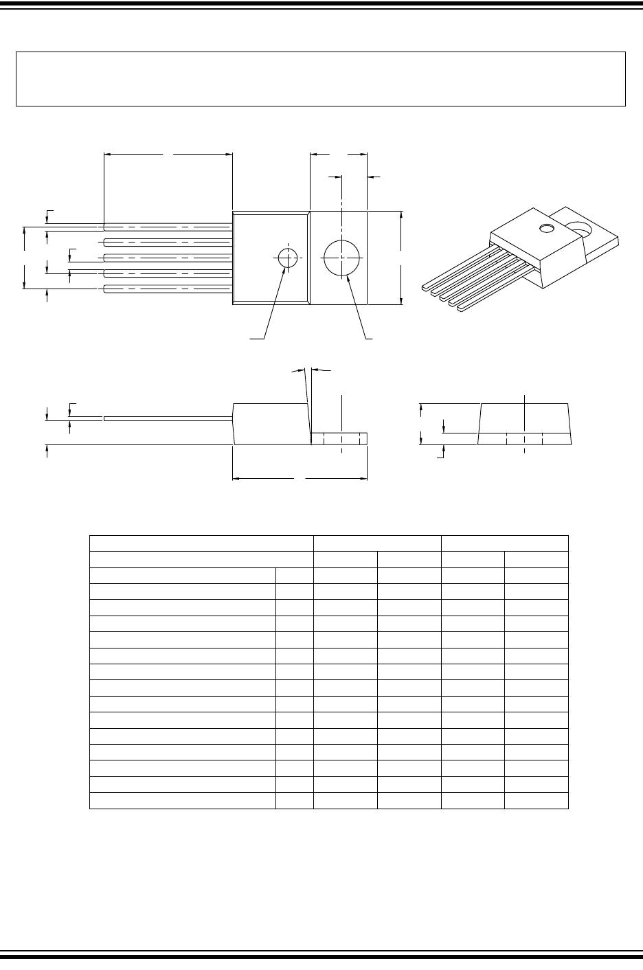
5-Lead TO-220
XXXXXXXXX
XXXXXXXXX
YYWWNNN
Example:
TC4421A
XXXXXXXXX
0514256
VAT^^
Legend: XX...X Customer-specific information
Y Year code (last digit of calendar year)
YY Year code (last 2 digits of calendar year)
WW Week code (week of January 1 is week ‘01’)
NNN Alphanumeric traceability code
Pb-free JEDEC designator for Matte Tin (Sn)
* This package is Pb-free. The Pb-free JEDEC designator ( )
can be found on the outer packaging for this package.
Note: In the event the full Microchip part number cannot be marked on one line, it will
be carried over to the next line, thus limiting the number of available
characters for customer-specific information.