MC100LVEP16DR2G

© Semiconductor Components Industries, LLC, 2016
August, 2016 Rev. 12
1 Publication Order Number:
MC10LVEP16/D
MC10LVEP16, MC100LVEP16
2.5V / 3.3V ECL
Differential Receiver/Driver
Description
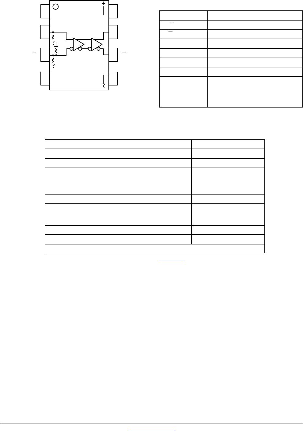
The MC10/100LVEP16 is a world class differential receiver/driver.
The device is functionally equivalent to the EL16, EP16 and LVEL16
devices. With output transition times significantly faster than the EL16
and LVEL16, the LVEP16 is ideally suited for interfacing with high
frequency and low voltage (2.5 V) sources. Single-Ended CLK input
operation is limited to a V
CC
3.0 V in PECL mode, or V
EE
3.0 V in
NECL mode.
The V
BB
pin, an internally generated Voltage supply, is available to
this device only. For Single-Ended input conditions, the unused
differential input is connected to V
BB
as a switching reference voltage.
V
BB
may also rebias AC coupled inputs. When used, decouple V
BB
and V
CC
via a 0.01 mF capacitor and limit current sourcing or sinking
to 0.5 mA. When not used, V
BB
should be left open.
The 100 Series contains temperature compensation.
Features
240 ps Propagation Delay
Maximum Frequency = > 4 GHz Typical
PECL Mode Operating Range:
V
CC
= 2.375 V to 3.8 V with V
EE
= 0 V
NECL Mode Operating Range:
V
CC
= 0 V with V
EE
= 2.375 V to 3.8 V
V
BB
Output
Open Input Default State
LVDS Input Compatible
These Devices are Pb-Free, Halogen Free and are RoHS Compliant
*For additional marking information, refer to
Application Note AND8002/D
.
H = MC10 A = Assembly Location
K = MC100 L = Wafer Lot
5Y = MC10 Y = Year
4L = MC100 W = Work Week
M = Date Code G = Pb-Free Package
(Note: Microdot may be in either location)
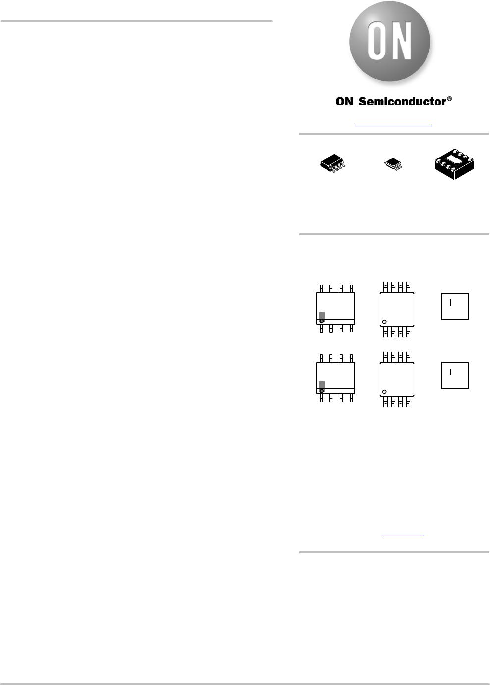
MARKING DIAGRAMS*
HU16
ALYWG
G
KU16
ALYWG
G
SOIC8 NB
D SUFFIX
CASE 75107
TSSOP8
DT SUFFIX
CASE 948R02
1
8
1
8
1
8
www.onsemi.com
See detailed ordering and shipping information in the package
dimensions section on page 9 of this data sheet.
ORDERING INFORMATION
1
8
HVP16
ALYW
G
1
8
KVP16
ALYW
G
1
8
DFN8
MN SUFFIX
CASE 506AA
5Y MG
G
14
4L MG
G
14
SOIC8 NB TSSOP8 DFN8
MC10LVEP16, MC100LVEP16
www.onsemi.com
2
1
2
3
45
6
7
8
Q
V
EE
V
CC
D
Q
D
V
BB
NC
Figure 1. 8-Lead Pinout (Top View) and Logic
Diagram
Table 1. PIN DESCRIPTION
Pin Function
D*, D** ECL Data Inputs
Q, Q ECL Data Outputs
V
BB
Ref. Voltage Output
V
CC
Positive Supply
V
EE
Negative Supply
NC No Connect
EP (DFN8 only) Thermal exposed pad must
be connected to a sufficient thermal con-
duit. Electrically connect to the most neg-
ative supply (GND) or leave unconnec-
ted, floating open.
* Pins will default LOW when left open.
**Pins will default to V
CC
/2 when left open.
Table 2. ATTRIBUTES
Characteristics Value
Internal Input Pulldown Resistor
75 kW
Internal Input Pullup Resistor
37.5 kW
ESD Protection
Human Body Model
Machine Model
Charged Device Model
> 4 kV
> 200 V
> 2 kV
Moisture Sensitivity, Indefinite Time Out of Drypack (Note 1) Pb-Free Pkg
SOIC8 NB NB
TSSOP8
DFN8
Level 1
Level 3
Level 1
Flammability Rating Oxygen Index: 28 to 34 UL 94 V0 @ 0.125 in
Transistor Count 167 Devices
Meets or exceeds JEDEC Spec EIA/JESD78 IC Latchup Test
1. For additional information, see Application Note AND8003/D.
MC10LVEP16, MC100LVEP16
www.onsemi.com
3
Table 3. MAXIMUM RATINGS
Symbol Parameter Condition 1 Condition 2 Rating Unit
V
CC
PECL Mode Power Supply V
EE
= 0 V 6 V
V
EE
NECL Mode Power Supply V
CC
= 0 V 6 V
V
I
PECL Mode Input Voltage
NECL Mode Input Voltage
V
EE
= 0 V
V
CC
= 0 V
V
I
V
CC
V
I
V
EE
6
6
V
I
out
Output Current Continuous
Surge
50
100
mA
I
BB
V
BB
Sink/Source ±0.5 mA
T
A
Operating Temperature Range 40 to +85 °C
T
stg
Storage Temperature Range 65 to +150 °C
q
JA
Thermal Resistance (Junction-to-Ambient) 0 lfpm
500 lfpm
SOIC8 NB
SOIC8 NB
190
130
°C/W
q
JC
Thermal Resistance (Junction-to-Case) Standard Board SOIC8 NB 41 to 44 °C/W
q
JA
Thermal Resistance (Junction-to-Ambient) 0 lfpm
500 lfpm
TSSOP8
TSSOP8
185
140
°C/W
q
JC
Thermal Resistance (Junction-to-Case) Standard Board TSSOP8 41 to 44 °C/W
q
JA
Thermal Resistance (Junction-to-Ambient) 0 lfpm
500 lfpm
DFN8
DFN8
129
84
°C/W
T
sol
Wave Solder (Pb-Free) < 2 to 3 sec @ 260°C 265 °C
q
JC
Thermal Resistance (Junction-to-Case) (Note 1) DFN8 35 to 40 °C/W
Stresses exceeding those listed in the Maximum Ratings table may damage the device. If any of these limits are exceeded, device functionality
should not be assumed, damage may occur and reliability may be affected.
1. JEDEC standard multilayer board 2S2P (2 signal, 2 power)

MC100LVEP16DR2G

Mfr. #:
Manufacturer:
ON Semiconductor
Description:
Bus Transceivers 2.5V/3.3V ECL Diff
Lifecycle:
New from this manufacturer.
Delivery:
DHL FedEx Ups TNT EMS
Payment:
T/T Paypal Visa MoneyGram Western Union