MC10LVEP16, MC100LVEP16
www.onsemi.com
7
Table 10. AC CHARACTERISTICS (V
CC
= 0 V; V
EE
= −3.8 V to −2.375 V or V
CC
= 2.375 V to 3.8 V; V
EE
= 0 V (Note 1))
Symbol
Characteristic
−40°C 25°C 85°C
Unit
Min Typ Max Min Typ Max Min Typ Max
f
max
Maximum Frequency
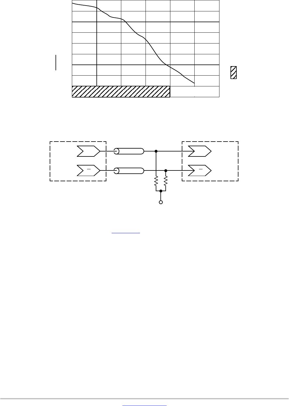
(See Figure 2. F
max
/JITTER)
> 4 > 4 > 4 GHz
t
PLH
,
t
PHL
Propagation Delay to
Output Differential
150 220 300 170 240 320 190 260 330 ps
t
SKEW
Duty Cycle Skew (Note 2) 5.0 20 5.0 20 5.0 20 ps
t
JITTER
CLOCK Random Jitter (RMS)
@ ≤ 1.0 GHz
@ ≤ 1.5 GHz
@ ≤ 2.0 GHz
@ ≤ 2.5 GHz
@ ≤ 3.0 GHz
@ ≤ 3.5 GHz
0.134
0.077
0.115
0.117
0.122
0.123
0.2
0.2
0.2
0.2
0.2
0.2
0.147
0.104
0.141
0.132
0.143
0.145
0.3
0.3
0.3
0.3
0.3
0.3
0.166
0.145
0.153
0.156
0.177
0.202
0.3
0.3
0.3
0.3
0.3
0.3
ps
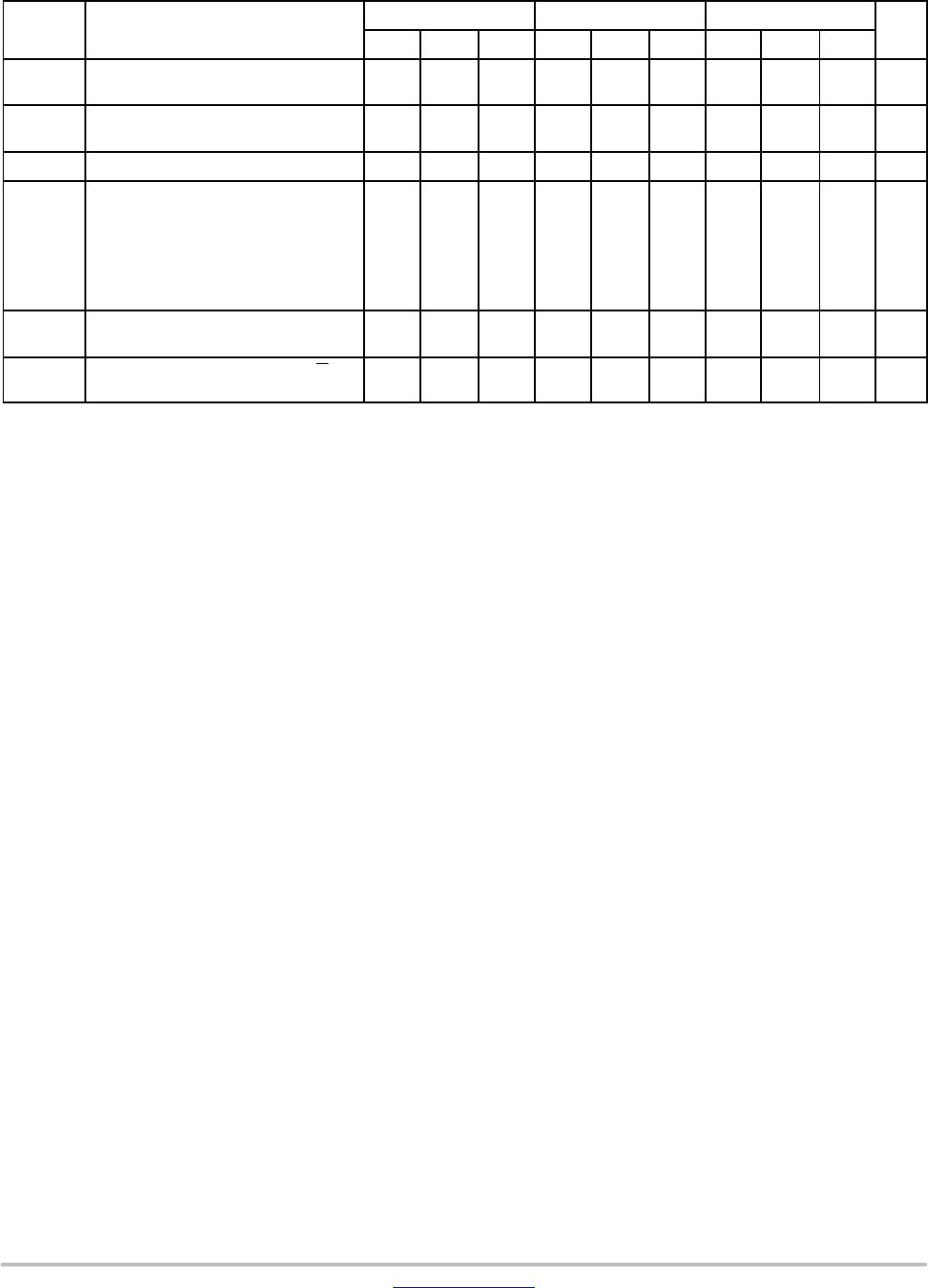
V
PP
Input Voltage Swing
(Differential Configuration)
150 800 1200 150 800 1200 150 800 1200 mV
t
r
t
f
Output Rise/Fall Times Q, Q
(20% − 80%)
70 120 170 80 130 180 100 150 200 ps
NOTE: Device will meet the specifications after thermal equilibrium has been established when mounted in a test socket or printed circuit
board with maintained transverse airflow greater than 500 lfpm. Electrical parameters are guaranteed only over the declared
operating temperature range. Functional operation of the device exceeding these conditions is not implied. Device specification limit
values are applied individually under normal operating conditions and not valid simultaneously.
1. Measured using a 750 mV source, 50% duty cycle clock source. All loading with 50 W to V
CC
− 2.0 V.
2. Skew is measured between outputs under identical transitions. Duty cycle skew is defined only for differential operation when the delays
are measured from the cross point of the inputs to the cross point of the outputs.